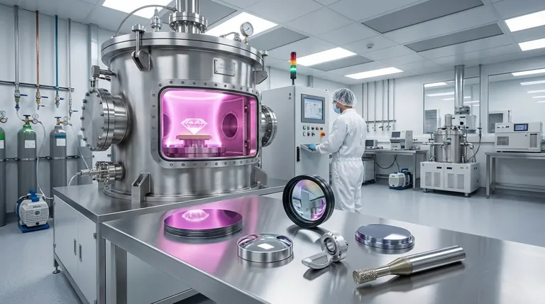
At its core, Microwave Plasma Chemical Vapor Deposition (MPCVD) is a foundational technology for industries requiring materials with extreme performance characteristics. It is most commonly used in electronics for semiconductors and heat sinks, high-performance optics, durable cutting tools, and advanced biomedical applications where material purity and structural perfection are non-negotiable.
The widespread adoption of MPCVD is not accidental. It stems from its unique ability to grow exceptionally pure, high-quality crystalline materials—most notably diamond—with a level of control and stability that other deposition methods cannot match.
The Core Advantage: Unmatched Purity and Control
The reason MPCVD is favored in demanding fields is its superior process environment. Unlike competing technologies, it creates the ideal conditions for near-perfect material growth.
Eliminating Contamination
A key advantage of MPCVD is its electrodeless nature. The plasma is generated by microwaves, meaning there are no internal components like filaments or electrodes that can erode and introduce impurities into the material being grown.
This results in a final product, such as a synthetic diamond, with exceptional chemical purity.
Achieving Stable, Controllable Growth
MPCVD allows for precise and independent control over critical process parameters like temperature, pressure, and gas composition.
This stability is crucial for consistently producing uniform, high-quality materials over large areas and for long deposition times, making it ideal for industrial-scale production.
Enabling Large, High-Quality Crystals
The combination of a clean, stable environment makes MPCVD the premier method for growing large, single-crystal diamonds.
This capability is essential for applications in high-power electronics and advanced optics, where material defects would severely degrade performance.
Key Industrial Applications Driven by MPCVD
The unique advantages of MPCVD directly enable its use in several high-technology sectors.
Electronics and Semiconductors
Diamond's thermal conductivity is the highest of any known material. MPCVD is used to create diamond heat spreaders for high-power density electronics, effectively cooling laser diodes, power transistors, and CPUs.
Its properties as an ultra-wide-bandgap semiconductor are also being exploited for next-generation radio-frequency and power-switching devices.
High-Performance Optics
MPCVD-grown diamond has an incredibly broad optical transmission window, from the ultraviolet to the far-infrared and microwave bands.
This makes it an ideal material for durable, high-performance windows, lenses, and domes used in harsh environments, such as in lasers, spectroscopy, and aerospace applications.
Cutting Tools and Abrasives
Applying a thin, uniform coating of MPCVD diamond onto cutting tools dramatically increases their hardness, wear resistance, and lifespan.
This is critical for machining highly abrasive materials like carbon fiber composites, ceramics, and non-ferrous metal alloys where traditional tools fail quickly.
Biomedical Applications
Diamond is inherently biocompatible and chemically inert. MPCVD is used to create coatings for medical implants to improve their longevity and reduce adverse reactions with the body.
Furthermore, diamond's unique electrochemical properties make it a superior material for creating highly sensitive and stable biosensors and medical electrodes.
Understanding the Trade-offs
While MPCVD is superior for high-quality applications, its choice over other CVD methods is a matter of strategic trade-offs.
Why Not Hot Filament CVD (HFCVD)?
HFCVD is a simpler, lower-cost method. However, its core limitation is the hot filament itself, which degrades over time and introduces contaminants (typically tungsten) into the diamond film, compromising purity and performance.
Why Not DC Arc Jet CVD?
DC Arc Jet systems can achieve very high growth rates. However, they are often less stable and can suffer from electrode erosion, leading to impurities and lower-quality polycrystalline material compared to the single-crystal capabilities of MPCVD.
Making the Right Choice for Your Application
The decision to use MPCVD is directly tied to the performance demands of the end product.
- If your primary focus is maximum material purity, single-crystal quality, and performance: MPCVD is the undisputed industry standard for applications like high-power electronics and optics.
- If your primary focus is lower cost or rapid coating of a large area where some impurity is acceptable: Methods like HFCVD or DC Arc Jet may be considered, but with a clear trade-off in final material quality.
Ultimately, selecting the right synthesis method requires aligning the technology's capabilities with the uncompromising demands of your specific application.
Summary Table:
| Industry | Key Applications | Benefits of MPCVD |
|---|---|---|
| Electronics | Semiconductors, heat spreaders | High thermal conductivity, purity for power devices |
| Optics | Windows, lenses, domes | Broad optical transmission, durability in harsh environments |
| Cutting Tools | Coatings for abrasives | Enhanced hardness, wear resistance, longer tool life |
| Biomedical | Implants, biosensors | Biocompatibility, chemical inertness, stability |
Unlock the full potential of MPCVD for your advanced applications with KINTEK! Leveraging exceptional R&D and in-house manufacturing, we provide tailored high-temperature furnace solutions, including our advanced CVD/PECVD systems, to meet your unique experimental needs. Whether you're in electronics, optics, or biomedical fields, our deep customization capabilities ensure precise performance. Contact us today to discuss how we can enhance your material synthesis and drive innovation in your industry!
Visual Guide

Related Products
- 915MHz MPCVD Diamond Machine Microwave Plasma Chemical Vapor Deposition System Reactor
- MPCVD Machine System Reactor Bell-jar Resonator for Lab and Diamond Growth
- Cylindrical Resonator MPCVD Machine System for Lab Diamond Growth
- Multi Heating Zones CVD Tube Furnace Machine for Chemical Vapor Deposition Equipment
- Inclined Rotary Plasma Enhanced Chemical Deposition PECVD Tube Furnace Machine
People Also Ask
- How does the MPCVD process work to deposit diamond? A Guide to High-Purity Synthesis
- What are the essential components of an MPCVD reactor for diamond film deposition? Unlock High-Quality Diamond Growth
- What is the basic principle of operation for the microwave plasma chemical vapor deposition system? Unlock High-Purity Material Growth
- What are some key features and benefits of the microwave plasma chemical vapor deposition system? Achieve Unmatched Material Synthesis
- What is the MPCVD method and why is it considered effective for diamond deposition? Superior Purity & High Growth Rates


