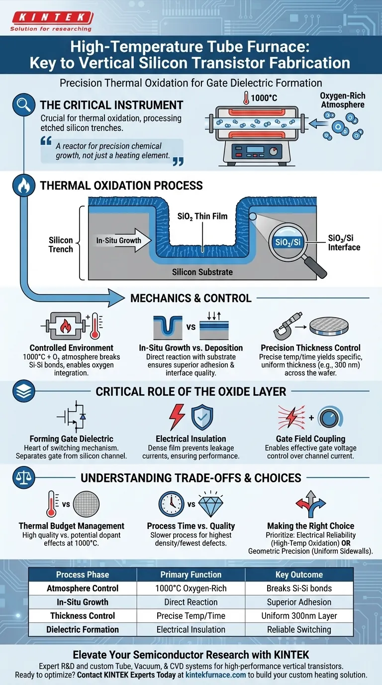
In the fabrication of vertical silicon transistors, the high-temperature tube furnace is the critical instrument used for thermal oxidation. Specifically, it is employed to process etched silicon trenches by exposing them to an oxygen-rich atmosphere at temperatures around 1000°C. This process facilitates the in-situ growth of a dense, high-quality Silicon Dioxide (SiO2) thin film directly onto the silicon sidewalls.
The furnace is not merely a heating element; it is a reactor for precision chemical growth. Its primary function is to transform the exposed silicon surface into a uniform, insulating oxide layer that serves as the gate dielectric, defining the transistor's electrical reliability.
The Mechanics of the Oxidation Process
Controlled High-Temperature Environment
The tube furnace creates a strictly controlled environment essential for high-quality oxidation.
By operating at approximately 1000°C in an oxygen-rich atmosphere, the furnace provides the thermal energy required to break silicon-silicon bonds and allow oxygen integration.
In-Situ Growth vs. Deposition
Unlike deposition methods where material is added on top, this process utilizes in-situ growth.
The oxygen reacts directly with the silicon substrate of the trench sidewalls. This consumes a portion of the silicon to create the new SiO2 layer, ensuring superior adhesion and interface quality.
Precision Thickness Control
The furnace allows for the creation of specific oxide thicknesses necessary for device specifications.
Through precise control of temperature and time, the process yields a specific film thickness, such as 300 nm. This thickness is critical for maintaining consistent electrical properties across the wafer.
The Critical Role of the Oxide Layer
Forming the Gate Dielectric
The Silicon Dioxide layer produced in the furnace functions as the gate dielectric for the vertical transistor.
This is the heart of the transistor's switching mechanism. A high-quality dielectric is required to separate the conductive gate from the silicon channel.
Electrical Insulation
The density of the film grown at high temperatures ensures robust electrical insulation.
A dense SiO2 film prevents leakage currents that would otherwise degrade the performance or efficiency of the transistor.
Gate Field Coupling
Beyond insulation, the oxide layer facilitates gate field coupling.
This allows the voltage applied to the gate to effectively control the flow of current within the vertical silicon channel, enabling the transistor to switch states efficiently.
Understanding the Trade-offs
Thermal Budget Management
Operating at 1000°C introduces a significant thermal budget to the fabrication process.
While high temperatures produce the highest quality oxides, they can negatively affect dopant profiles or other materials already present on the wafer.
Process Time and Throughput
Growing a thick oxide layer (such as 300 nm) via thermal oxidation is a relatively slow process.
This method prioritizes film quality and density over processing speed. If high throughput is the only metric, alternative deposition methods might be faster, but they typically result in lower-quality films with poorer electrical interfaces.
Making the Right Choice for Your Goal
When integrating a tube furnace for vertical transistor fabrication, consider your specific device requirements:
- If your primary focus is electrical reliability: Prioritize this high-temperature thermal oxidation method, as the in-situ growth creates the highest density film with the fewest defects.
- If your primary focus is geometric precision: Rely on this method to ensure the gate dielectric forms uniformly on vertical sidewalls, utilizing the silicon trench itself as the foundation for the oxide.
Success in vertical transistor fabrication relies on accepting the thermal demands of the tube furnace to achieve the superior dielectric integrity required for device performance.
Summary Table:
| Process Phase | Primary Function | Key Outcome |
|---|---|---|
| Atmosphere Control | 1000°C Oxygen-rich environment | Breaks Si-Si bonds for oxygen integration |
| In-Situ Growth | Direct reaction with trench sidewalls | Superior adhesion and interface quality |
| Thickness Control | Precise temp/time regulation | Uniform 300nm gate dielectric layers |
| Dielectric Formation | Electrical insulation & coupling | Reliable transistor switching & zero leakage |
Elevate Your Semiconductor Research with KINTEK
High-performance vertical transistors demand uncompromising thermal precision. Backed by expert R&D and manufacturing, KINTEK offers specialized Tube, Vacuum, and CVD systems designed for the rigorous demands of silicon substrate processing. Our high-temperature furnaces are fully customizable to your unique thermal budget and oxidation requirements.
Ready to optimize your gate dielectric quality?
Contact KINTEK Experts Today — Let us build the custom heating solution your lab needs.
Visual Guide
References
- Quanyang Tao, Yuan Liu. High-density vertical sidewall MoS2 transistors through T-shape vertical lamination. DOI: 10.1038/s41467-024-50185-4
This article is also based on technical information from Kintek Furnace Knowledge Base .
Related Products
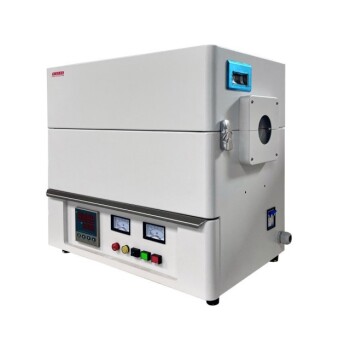
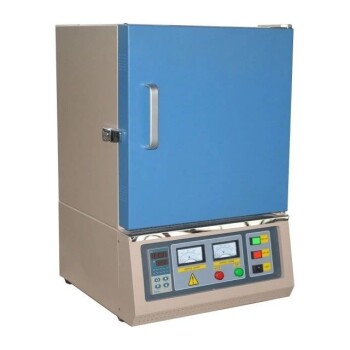
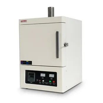
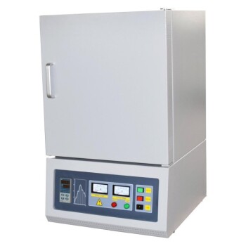
- 1700℃ High Temperature Laboratory Tube Furnace with Alumina Tube
- 1400℃ High Temperature Laboratory Tube Furnace with Alumina Tube
- Vertical Laboratory Quartz Tube Furnace Tubular Furnace
- 1200℃ Split Tube Furnace Laboratory Quartz Tube Furnace with Quartz Tube
- 1400℃ Muffle Oven Furnace for Laboratory
People Also Ask
- What is a high temperature tube furnace? Achieve Precise Heat and Atmosphere Control
- How does a laboratory high-temperature tube furnace contribute to the conversion of electrospun fibers? Expert Insights
- What factors should be considered when selecting a high temperature tube furnace? Ensure Precision and Reliability for Your Lab
- What role do high-performance box or tube furnaces play in LATP sintering? Master Densification & Ionic Conductivity
- What is the function of a furnace in CuAlMn alloy treatment? Achieve Perfect Microstructural Homogenization