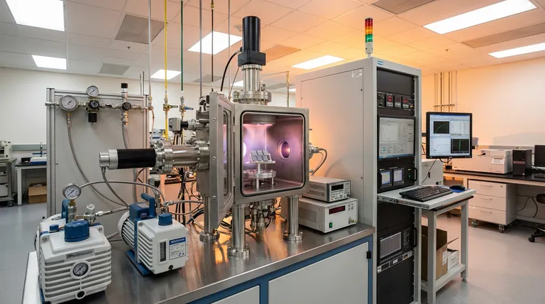
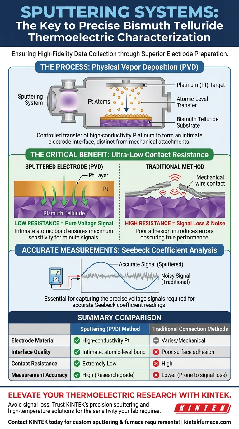
A sputtering system serves as a critical tool for ensuring high-fidelity data collection during the thermoelectric characterization of Bismuth Telluride. By utilizing physical vapor deposition (PVD) technology, the system deposits high-conductivity Platinum (Pt) electrodes directly onto the sample surface. This process creates a superior electrical interface compared to standard connection techniques, which is fundamental for accurate voltage measurements.
By significantly lowering contact resistance through precise Platinum deposition, sputtering systems ensure the sensitivity required to accurately capture voltage signals for Seebeck coefficient analysis.
The Process of Electrode Formation
Physical Vapor Deposition (PVD)
The sputtering system operates on the principle of Physical Vapor Deposition.
This advanced technology allows for the controlled transfer of material from a source to a substrate at the atomic level.
In the context of Bismuth Telluride characterization, this method is used to construct the electrode interface rather than simply attaching wires mechanically.
Platinum (Pt) Deposition
The system specifically deposits Platinum (Pt) onto the Bismuth Telluride samples.
Platinum is selected for its high conductivity and stability.
By coating the sample with this specific metal, the system establishes a highly conductive pathway necessary for subsequent electrical testing.
The Criticality of Low Contact Resistance
Superior Interface Quality
The primary advantage of using a sputtering system is the dramatic reduction in contact resistance.
Electrodes prepared via sputtering form an intimate, low-resistance interface with the Bismuth Telluride surface.
This contrasts sharply with traditional connection methods, which often suffer from higher resistance due to poor surface adhesion or material mismatch.
Ensuring Measurement Sensitivity
Low contact resistance is not merely a structural feature; it directly dictates measurement accuracy.
In thermoelectric characterization, particularly when measuring the Seebeck coefficient, the system must capture minute voltage signals.
A high-resistance interface would introduce noise or voltage drops, obscuring the true performance of the material. Sputtering ensures the voltage signal remains pure and sensitive.
Understanding the Trade-offs
Sputtering vs. Traditional Methods
While sputtering provides superior data, it is important to understand why it is compared against "traditional connection methods."
Traditional methods may be faster or require less equipment, but they compromise the integrity of the electrical contact.
The trade-off for the high accuracy provided by sputtering is the requirement for specialized PVD equipment, but this is a necessary investment for avoiding the signal loss associated with simpler manual connections.
Making the Right Choice for Your Goal
To maximize the quality of your thermoelectric analysis, consider the following recommendations:
- If your primary focus is High-Precision Characterization: Prioritize the use of a sputtering system to deposit Platinum electrodes, as this guarantees the low contact resistance required for accurate Seebeck coefficient readings.
- If your primary focus is Avoiding Signal Loss: Avoid traditional connection methods, which create inferior interfaces that can degrade voltage signal sensitivity.
Using a sputtering system is the definitive method for transforming Bismuth Telluride samples into testable devices with research-grade accuracy.
Summary Table:
| Feature | Sputtering (PVD) Method | Traditional Connection Methods |
|---|---|---|
| Electrode Material | High-conductivity Platinum (Pt) | Varies (Mechanical/Adhesive) |
| Interface Quality | Intimate, atomic-level bond | Poor surface adhesion |
| Contact Resistance | Extremely Low | High |
| Measurement Accuracy | High (Research-grade) | Lower (Prone to signal loss) |
| Primary Benefit | Precise Seebeck coefficient analysis | Lower equipment requirement |
Elevate Your Thermoelectric Research with Precision Sputtering
Precise material characterization starts with a superior electrical interface. At KINTEK, we understand that accurate data collection for Bismuth Telluride depends on high-quality electrode deposition. Backed by expert R&D and manufacturing, we offer a comprehensive range of lab equipment—including Muffle, Tube, Rotary, Vacuum, and CVD systems—all customizable to meet your unique research needs.
Don't let high contact resistance compromise your Seebeck coefficient analysis. Trust KINTEK’s high-temperature and vacuum solutions to deliver the sensitivity your lab requires.
Contact KINTEK today to discuss your custom sputtering and furnace requirements!
Visual Guide
References
- N.G. Imam, Abd El‐Hady B. Kashyout. Comprehensive study of nanostructured Bi <sub>2</sub> Te <sub>3</sub> thermoelectric materials – insights from synchrotron radiation XRD, XAFS, and XRF techniques. DOI: 10.1039/d3ra06731a
This article is also based on technical information from Kintek Furnace Knowledge Base .
Related Products
- Spark Plasma Sintering SPS Furnace
- HFCVD Machine System Equipment for Drawing Die Nano Diamond Coating
People Also Ask
- What is the significance of high-precision temperature monitoring systems in SPS? Control Ti-6Al-4V/HA Microstructure
- What is unique about the heating mechanism of a Spark Plasma Sintering (SPS) furnace when preparing nanostructured h-BN ceramics? Achieve Ultra-Fast Densification and Suppress Grain Growth
- What are the advantages of spark plasma sintering (SPS) over traditional forging? Precision Microstructural Control
- What are the advantages of using a Spark Plasma Sintering (SPS) furnace? Achieve Rapid Densification and High ZT
- What are the steps in the discharge plasma sintering process? Master Fast, High-Density Material Consolidation

