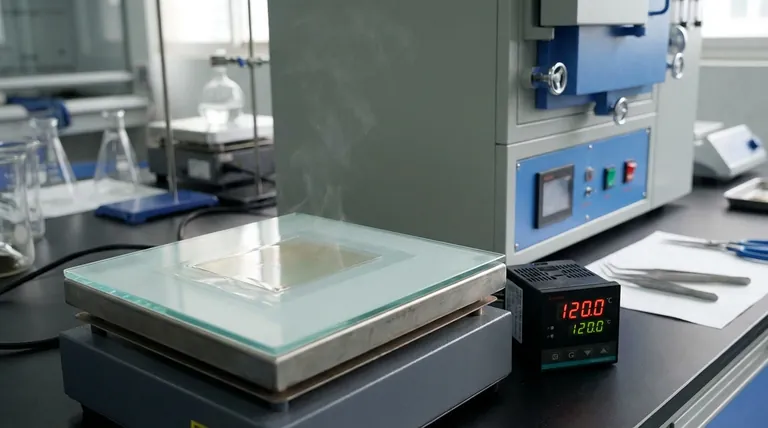
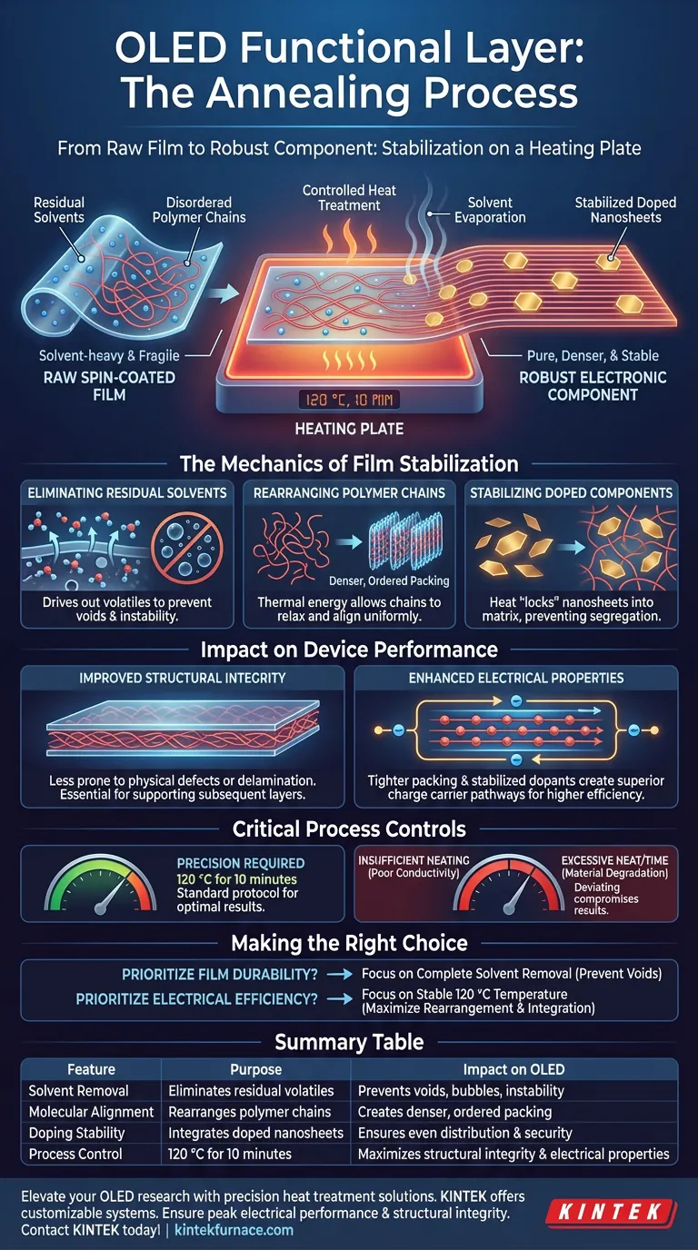
The annealing process is a critical stabilization step designed to transform a raw, spin-coated film into a robust electronic component. By subjecting the heating plate to a controlled temperature—typically 120 °C for 10 minutes—you effectively drive out residual solvents and force the material's internal structure to settle into a more efficient configuration.
Annealing serves as the bridge between physical deposition and electronic functionality. It solidifies the film’s structure by removing volatile liquids and aligning the molecular components for optimal electrical performance.
The Mechanics of Film Stabilization
Eliminating Residual Solvents
Spin-coating is an effective deposition method, but it inherently leaves residual solvents trapped within the thin film.
If left untreated, these solvents can cause voids, bubbles, or chemical instability over time.
Annealing provides the thermal energy necessary to evaporate these volatiles completely, leaving behind a pure functional layer.
Rearranging Polymer Chains
The heat treatment does more than just dry the film; it promotes the rearrangement of polymer chains.
The thermal energy allows the polymer molecules to relax and align themselves more uniformly.
This reorganization reduces internal stress within the film and creates a denser, more ordered molecular packing.
Stabilizing Doped Components
For layers containing additives, the process stabilizes the integration of doped nanosheets.
Heat helps "lock" these nanosheets into the polymer matrix, preventing segregation or loose binding.
This ensures that the dopants are evenly distributed and mechanically secured within the layer.
Impact on Device Performance
Improved Structural Integrity
By removing solvents and aligning the molecular structure, annealing significantly enhances the structural integrity of the layer.
A stable, solid film is less prone to physical defects or delamination.
This robustness is essential for supporting subsequent layers in the OLED stack.
Enhanced Electrical Properties
The microscopic reorganization directly translates to better electrical properties.
Tighter molecular packing and stabilized dopants create superior pathways for charge carriers.
This results in a more efficient functional layer capable of sustaining the necessary current for OLED operation.
Critical Process Controls
Adhering to Specific Parameters
The benefits of annealing rely heavily on controlled heat treatment.
The standard protocol of 120 °C for 10 minutes is specific; deviating from this can compromise the results.
The Risk of Improper Heating
Insufficient heating may leave solvents behind, leading to poor conductivity.
Conversely, excessive heat or time could degrade the sensitive organic polymers or nanosheets.
Precision is required to balance solvent removal with material preservation.
Making the Right Choice for Your Goal
To maximize the effectiveness of your OLED functional layers, consider your primary objective:
- If your primary focus is Film Durability: prioritize the complete removal of residual solvents to prevent voids and physical defects in the final device.
- If your primary focus is Electrical Efficiency: ensure the temperature remains stable at 120 °C to facilitate maximum polymer chain rearrangement and nanosheet integration.
Successful annealing turns a fragile, solvent-heavy coating into a high-performance foundation for your OLED device.
Summary Table:
| Feature | Purpose | Impact on OLED |
|---|---|---|
| Solvent Removal | Eliminates residual volatiles | Prevents voids, bubbles, and chemical instability |
| Molecular Alignment | Rearranges polymer chains | Creates denser, more ordered molecular packing |
| Doping Stability | Integrates doped nanosheets | Ensures even distribution and mechanical security |
| Process Control | 120 °C for 10 minutes | Maximizes structural integrity and electrical properties |
Elevate your OLED research with precision heat treatment solutions. Backed by expert R&D and manufacturing, KINTEK offers Muffle, Tube, Rotary, Vacuum, and CVD systems, all fully customizable to meet your unique functional layer requirements. Ensure your films achieve peak electrical performance and structural integrity with our high-temp lab furnaces. Contact KINTEK today to find the perfect system for your lab!
Visual Guide
References
- Dipanshu Sharma, Jwo‐Huei Jou. Two-Dimensional Transition Metal Dichalcogenide: Synthesis, Characterization, and Application in Candlelight OLED. DOI: 10.3390/molecules30010027
This article is also based on technical information from Kintek Furnace Knowledge Base .
Related Products
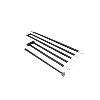
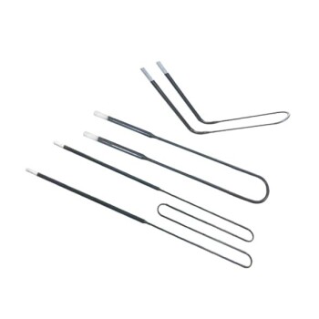
- Silicon Carbide SiC Thermal Heating Elements for Electric Furnace
- Molybdenum Disilicide MoSi2 Thermal Heating Elements for Electric Furnace
- Laboratory Quartz Tube Furnace RTP Heating Tubular Furnace
- Multi Heating Zones CVD Tube Furnace Machine for Chemical Vapor Deposition Equipment
- Split Multi Heating Zone Rotary Tube Furnace Rotating Tube Furnace
People Also Ask
- What are some common types of silicon carbide heating elements? Explore Shapes, Coatings, and High-Temp Performance
- What are the temperature capabilities and mounting options for silicon carbide heating elements? Unlock High-Temp Flexibility and Durability
- What are the advantages of using silicon carbide heating elements in industrial furnaces? Boost Efficiency and Durability
- What is the recommended surface load for silicon carbide heating elements at different furnace temperatures? Maximize Lifespan & Performance
- How do the different types of silicon carbide heating elements compare in terms of applications? Find the Best Fit for Your High-Temp Needs