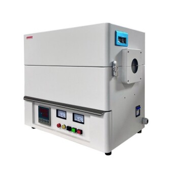
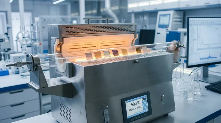
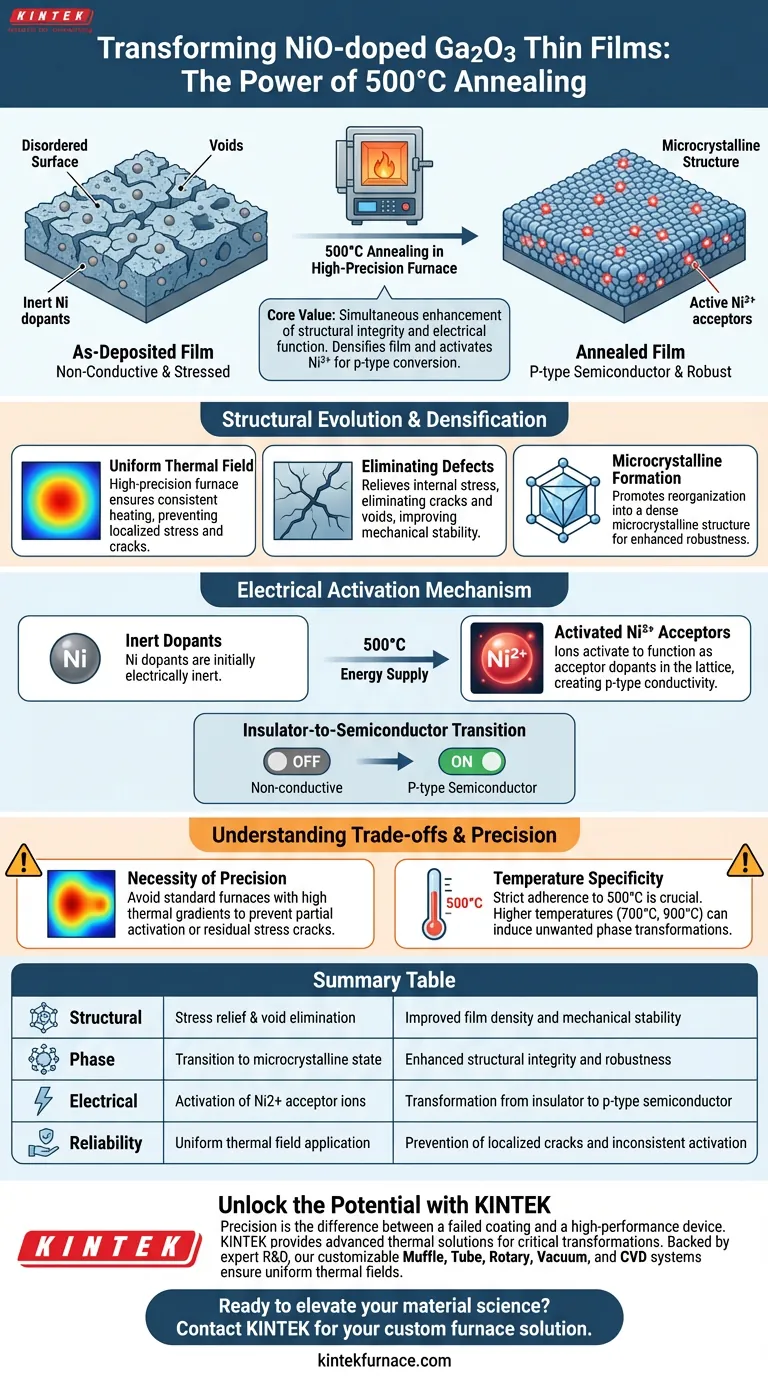
Annealing NiO-doped Ga2O3 thin films at 500°C triggers a critical transformation in both physical structure and electrical performance. This thermal treatment utilizes a high-precision furnace to repair deposition defects while simultaneously activating the material's semiconductor capabilities.
The core value of this process is the simultaneous enhancement of structural integrity and electrical function: it densifies the film by eliminating stress-induced voids and activates Ni2+ ions to convert a non-conductive layer into a functional p-type semiconductor.
Structural Evolution and Densification
The Role of Thermal Uniformity
Using a high-precision furnace is essential to establish a uniform thermal field.
Inconsistent heating can lead to localized stress points. A precise thermal environment ensures that the entire film undergoes the same physical changes simultaneously.
Eliminating Deposition Defects
Films often suffer from stress caused during the deposition phase.
The 500°C annealing process effectively relieves this internal stress. This results in the elimination of cracks and voids, significantly improving the mechanical stability of the layer.
Microcrystalline Formation
The thermal energy provided at this temperature promotes the organization of the material structure.
The film shifts toward a microcrystalline structure. This reorganization increases the overall film density, creating a more robust material compared to the as-deposited state.
Electrical Activation Mechanism
Activating the Dopant
Before annealing, the Nickel dopants may remain electrically inert.
The 500°C treatment supplies the energy required to activate Ni2+ ions. These ions begin to function as acceptor dopants within the crystal lattice.
The Insulator-to-Semiconductor Transition
The most significant functional change is the alteration of conductivity.
By activating the acceptors, the annealing process converts the initially non-conductive film into a high-performance p-type semiconductor. This is the critical step for enabling the material's use in electronic devices.
Understanding the Trade-offs
The Necessity of Precision
While the primary reference highlights the benefits, it implicitly underscores the need for equipment precision.
Standard furnaces with high thermal gradients may fail to produce the uniform field described. Without this uniformity, you risk partial activation or residual stress cracks in specific zones of the film.
Temperature Specificity
It is crucial to adhere strictly to the target temperature for this specific material system.
Supplementary data indicates that higher temperatures (e.g., 700°C or 900°C) can induce different phase transformations, such as converting materials to amorphous structures or altering bandgaps in iron-based oxides. For NiO-doped Ga2O3, 500°C is the calibrated point for achieving the desired microcrystalline p-type state.
Making the Right Choice for Your Goal
To maximize the utility of your NiO-doped Ga2O3 films, align your process controls with your specific end-goals:
- If your primary focus is Physical Durability: Ensure your furnace provides a strictly uniform thermal field to maximize density and eliminate void formation.
- If your primary focus is Electrical Conductivity: Verify that the 500°C dwell time is sufficient to fully activate the Ni2+ acceptors for p-type conversion.
Precision in thermal treatment is the bridge between a raw deposited coating and a high-performance semiconductor device.
Summary Table:
| Impact Category | Physical/Electrical Change | Resulting Benefit |
|---|---|---|
| Structural | Stress relief & void elimination | Improved film density and mechanical stability |
| Phase | Transition to microcrystalline state | Enhanced structural integrity and robustness |
| Electrical | Activation of Ni2+ acceptor ions | Transformation from insulator to p-type semiconductor |
| Reliability | Uniform thermal field application | Prevention of localized cracks and inconsistent activation |
Unlock the Potential of Your Semiconductor Materials
Precision is the difference between a failed coating and a high-performance electronic device. KINTEK provides the advanced thermal solutions necessary to achieve critical material transformations like the 500°C annealing of NiO-doped Ga2O3.
Backed by expert R&D and world-class manufacturing, KINTEK offers a comprehensive range of Muffle, Tube, Rotary, Vacuum, and CVD systems. Our high-temp lab furnaces are fully customizable to meet your unique research or production needs, ensuring the uniform thermal fields required for dopant activation and densification.
Ready to elevate your material science? Contact KINTEK today to find your custom furnace solution.
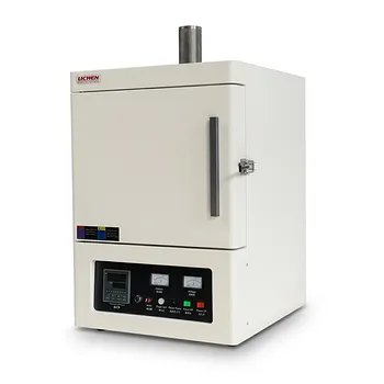
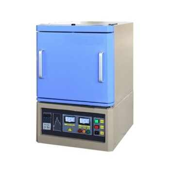
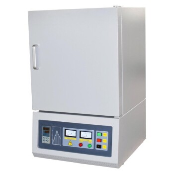
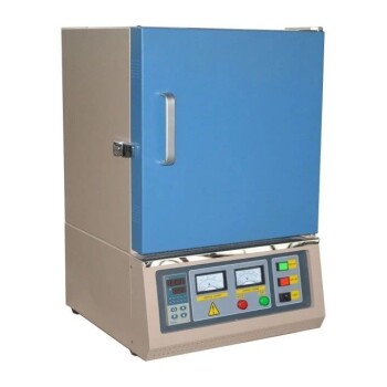
Visual Guide
References
- Cheng‐Fu Yang, Shu‐Han Liao. Analyses of the Properties of the NiO-Doped Ga2O3 Wide-Bandgap Semiconductor Thin Films. DOI: 10.3390/coatings14121615
This article is also based on technical information from Kintek Furnace Knowledge Base .
Related Products
- High Pressure Laboratory Vacuum Tube Furnace Quartz Tubular Furnace
- 1400℃ High Temperature Laboratory Tube Furnace with Alumina Tube
- 1700℃ High Temperature Laboratory Tube Furnace with Alumina Tube
- High Temperature Muffle Oven Furnace for Laboratory Debinding and Pre Sintering
- 1200℃ Muffle Oven Furnace for Laboratory
People Also Ask
- How does a laboratory tube furnace achieve controlled atmosphere sintering? Master Precision Catalytic Prep
- Why is control of heating rate and gas flow in a lab tube furnace critical for EM wave absorption materials?
- What role does a laboratory tube furnace play in the carbonization process of porous carbon particles? Expert Insights
- What are the different types of tube furnaces available? Find the Perfect Fit for Your Lab's Needs
- What are the main advantages of vacuum tube furnaces in the market? Achieve Purity and Precision in Material Processing