The fundamental necessity for this process is conductivity. Because graphitic carbon nitride (g-C3N4) is a semiconducting material, it lacks the inherent conductivity required to dissipate the electrons used during Scanning Electron Microscopy (SEM). Depositing a thin metal film creates a conductive path that prevents charge accumulation, while the vacuum environment ensures this layer is uniform, pure, and adhesive.
Core Takeaway Direct SEM imaging of g-C3N4 causes "charging," where trapped electrons distort the image and obscure surface details. Vacuum deposition applies a nanometer-thin metal layer (like Platinum) to drain this charge, enabling high-resolution visualization without altering the underlying morphology.
The Physics of the Problem: Charge Accumulation
The Conductivity Gap
SEM operates by bombarding a sample with a focused beam of high-energy electrons. For a clear image, these electrons must interact with the surface and then be conducted away to a ground.
The "Charging" Phenomenon
Since g-C3N4 is semiconducting, it cannot effectively drain these electrons. Consequently, electrons accumulate on the surface of the film.
Impact on Image Quality
This accumulation creates a negative electric field that repels the incoming electron beam. This results in severe image distortion, often manifesting as bright artifacts, drifting, or a total loss of resolution.
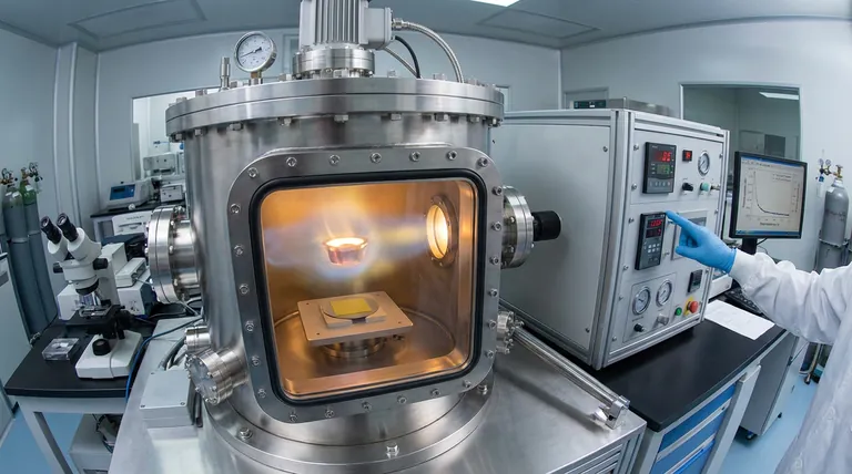
The Solution: Thin Film Deposition
Restoring Conductivity
To fix this, a layer of metal (often Platinum, Gold, or Aluminum) is deposited onto the sample. This layer creates a bridge for electrons to flow from the sample surface to the ground, effectively eliminating charging effects.
Preserving True Morphology
The metal layer is deposited to be only a few nanometers thick. This extreme thinness allows you to image the morphology and cross-section of the g-C3N4 without the metal coating masking the fine structural details.
Why Vacuum Equipment is Non-Negotiable
Eliminating Impurities
Vacuum evaporation or electron beam evaporation occurs in an environment void of air and residual gases. This prevents oxide layers or atmospheric impurities from forming between the metal and the g-C3N4 surface.
Ensuring Uniformity and Adhesion
In a high vacuum, metal atoms travel in a straight line (due to a long mean free path) without colliding with gas molecules. This ensures the metal bonds tightly to the film surface and forms a uniform, continuous coating, which is critical for consistent imaging.
Understanding the Trade-offs
Risk of Masking Features
While necessary, the metal coating physically covers the sample. If the deposition is not monitored precisely and the layer becomes too thick, it can obscure nanometer-scale features on the g-C3N4 surface.
Grain Size Interference
The metal film itself has a grain structure. At extremely high magnifications, you may inadvertently image the grains of the Platinum coating rather than the texture of the carbon nitride beneath it.
Making the Right Choice for Your Goal
When preparing g-C3N4 samples, the deposition parameters depend heavily on your specific analytical needs.
- If your primary focus is High-Resolution Imaging: Prioritize an extremely thin coating (1-3 nm) using fine-grain metals like Platinum to prevent charging without hiding surface details.
- If your primary focus is Electrical Characterization: Focus on the vacuum quality to ensure high purity and strong adhesion, which are essential for establishing reliable Ohmic or Schottky contacts.
Correct sample preparation transforms a non-conductive obstacle into a clear, high-fidelity window into your material's structure.
Summary Table:
| Feature | Impact on SEM Imaging | Role of Vacuum Deposition |
|---|---|---|
| Conductivity | Low conductivity causes electron "charging" and image distortion. | Provides a conductive path to drain electrons safely to ground. |
| Layer Purity | Atmospheric oxides interfere with image clarity and adhesion. | High vacuum ensures a pure, contaminant-free metal-to-sample bond. |
| Morphology | Thick coatings can mask nanometer-scale surface features. | Enables nanometer-thin, uniform layers that preserve true structure. |
| Adhesion | Poorly bonded films can flake under the electron beam. | Straight-line atom travel in vacuum ensures a continuous, tight bond. |
Enhance Your SEM Research with Precision Coating Solutions
Don't let sample charging compromise your g-C3N4 research. KINTEK provides industry-leading vacuum deposition systems designed specifically for advanced materials science. Backed by expert R&D and manufacturing, we offer high-performance Muffle, Tube, Rotary, Vacuum, and CVD systems—all fully customizable to meet your unique laboratory requirements.
Ready to achieve high-fidelity imaging results?
Contact KINTEK today to discuss your custom furnace and deposition needs
References
- Kota Higuchi, Yoshio Hashimoto. Layered carbon nitride films deposited under an oxygen-containing atmosphere and their electronic properties. DOI: 10.1063/5.0193419
This article is also based on technical information from Kintek Furnace Knowledge Base .
Related Products
- Stainless Steel Quick Release Vacuum Chain Three Section Clamp
- Vacuum Induction Melting Furnace
- 304 316 Stainless Steel High Vacuum Ball Stop Valve for Vacuum Systems
- Vacuum Hot Press Furnace Machine Heated Vacuum Press
- Vacuum Hot Press Furnace Machine for Lamination and Heating
People Also Ask
- What role do vacuum-sealed high-purity silica ampoules play in phase equilibrium experiments? Enhance Sample Integrity
- Why is a vacuum suction system required during the exhaust stage of rice straw-based charcoal carbonization?
- What is the function of quartz vacuum encapsulation in RhSeCl CVT? Mastering Pure Crystal Growth
- What is the function of PTFE sealing rings in plastic pyrolysis? Ensure Safe, Anaerobic Material Decomposition
- What is the operating principle of a vacuum freeze-dryer in the fabrication of carbon aerogels? Master Sublimation