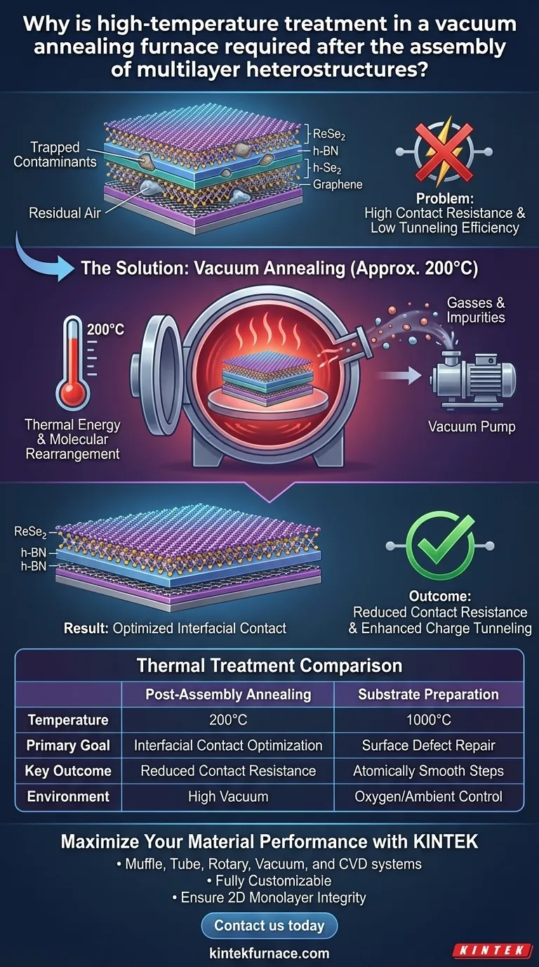
Post-assembly vacuum annealing is a critical purification step used to eliminate contaminants trapped between the layers of a heterostructure. By heating the device—typically to around 200°C—in a vacuum environment, you effectively drive out residual air and impurities, forcing the two-dimensional materials into closer physical contact.
The primary objective of this treatment is to optimize the interfacial contact between layers. By removing trapped residues and inducing molecular rearrangement, the process significantly reduces contact resistance and enhances the charge tunneling efficiency essential for high-performance devices.
The Mechanism of Interfacial Improvement
Removal of Trapped Contaminants
During the physical stacking or assembly of multilayer heterostructures (such as ReSe2/h-BN/Graphene), microscopic pockets of residual air and impurities inevitably become trapped between the layers.
If left untreated, these contaminants act as barriers. They prevent the atomic layers from achieving the intimate contact required for quantum phenomena to function correctly.
Thermal Expansion and Molecular Rearrangement
The annealing process typically involves heating the structure to approximately 200°C for two hours.
This introduction of thermal energy causes thermal expansion and induces molecular rearrangement within the heterostructure. As the materials expand and shift slightly, trapped gasses are expelled into the vacuum, and the layers settle into a more thermodynamically stable, flatter configuration.
Enhancement of Electrical Properties
The direct result of a cleaner, closer interface is a dramatic improvement in electrical performance.
Specifically, this process lowers contact resistance, ensuring that current flows smoothly across the junction. Furthermore, for vertical devices, the removal of interfacial gaps significantly boosts charge tunneling efficiency, which is often the limiting factor in device speed and sensitivity.
Understanding the Trade-offs: Process Temperature
It is vital to distinguish between post-assembly annealing and substrate preparation, as "high temperature" means different things in different contexts.
The Risk of Excessive Heat
For a fully assembled heterostructure, "high temperature" is relatively moderate (e.g., 200°C). Exceeding this range significantly can damage the delicate 2D monolayers or cause unwanted chemical reactions between the stack components.
Distinguishing Substrate Treatment
In contrast, substrate preparation requires much higher temperatures before any device assembly takes place.
As noted in substrate processing protocols, base materials often undergo annealing at 1000°C in oxygen. This extreme heat is necessary to remove organic contaminants, repair surface defects, and create atomically smooth step structures for epitaxial growth. However, this temperature is generally destructive to a finished multilayer heterostructure and must be applied only to the bare substrate.
Making the Right Choice for Your Goal
To ensure optimal device performance, you must apply the correct thermal treatment at the correct stage of fabrication.
- If your primary focus is optimizing a finished device: Utilize a moderate vacuum anneal (approx. 200°C) to expel trapped air and improve the electrical interface between stacked layers.
- If your primary focus is material growth quality: Utilize a high-temperature anneal (approx. 1000°C) on the bare substrate before assembly to ensure an atomically smooth nucleation surface.
Success relies on using thermal energy to clean the interface without compromising the structural integrity of the delicate 2D layers.
Summary Table:
| Feature | Post-Assembly Annealing | Substrate Preparation |
|---|---|---|
| Temperature | Approx. 200°C | Approx. 1000°C |
| Primary Goal | Interfacial Contact Optimization | Surface Defect Repair |
| Key Outcome | Reduced Contact Resistance | Atomically Smooth Steps |
| Environment | High Vacuum | Oxygen/Ambient Control |
Maximize Your Material Performance with KINTEK
Precise thermal control is the difference between a high-performance device and a failed experiment. Whether you need moderate-temperature vacuum annealing to perfect your heterostructure interfaces or high-heat systems for substrate preparation, KINTEK provides the solution.
Backed by expert R&D and manufacturing, we offer a wide range of Muffle, Tube, Rotary, Vacuum, and CVD systems, all fully customizable for your unique lab requirements. Ensure the integrity of your 2D monolayers and achieve superior charge tunneling efficiency today.
Ready to elevate your research? Contact us today to find the perfect furnace for your application!
Visual Guide
References
- Wei Li, Shaoxi Wang. Reconfigurable Floating‐Gate Devices with Ambipolar ReSe<sub>2</sub> Channel: Dual‐Mode Storage, NMOS‐PMOS Transformation, Logic Functions, Synapse Simulations, Positive and Negative Photoconductive Effects. DOI: 10.1002/adfm.202425359
This article is also based on technical information from Kintek Furnace Knowledge Base .
Related Products
- Vacuum Heat Treat Sintering and Brazing Furnace
- Small Vacuum Heat Treat and Tungsten Wire Sintering Furnace
- Vacuum Sealed Continuous Working Rotary Tube Furnace Rotating Tube Furnace
- Vacuum Heat Treat Sintering Furnace Molybdenum Wire Vacuum Sintering Furnace
- Vacuum Heat Treat Sintering Furnace with Pressure for Vacuum Sintering
People Also Ask
- What are the technical advantages of using Ti-35Ni-25Nb foil? High toughness and beta-phase stability.
- What are the advantages of using a vacuum heat treatment furnace? Achieve Superior Material Quality and Control
- What is the temperature of a vacuum furnace brazing? Optimize Your Joint Strength and Cleanliness
- How does vacuum heat treating affect the grain structure of metal alloys? Achieve Precise Microstructure Control
- What are the benefits of using vacuum heat treating furnaces for metal alloys? Achieve Superior Metal Properties and Performance


