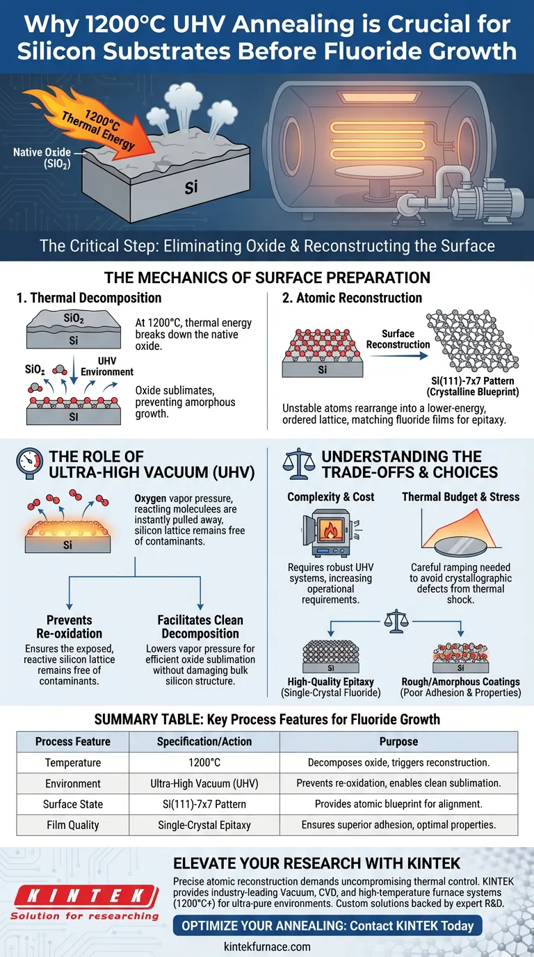
A high-temperature treatment at 1200°C is the critical preparation step required to completely eliminate the native oxide layer from a silicon substrate. This process utilizes thermal decomposition to strip away surface contaminants, exposing the pristine silicon atomic lattice underneath.
The process is not merely about cleaning; it is about architectural preparation. The 1200°C thermal treatment removes the oxide barrier to trigger surface reconstruction, specifically creating the Si(111)-7x7 pattern that serves as the necessary blueprint for high-quality epitaxial fluoride growth.
The Mechanics of Surface Preparation
Thermal Decomposition of Native Oxide
Silicon naturally forms a thin layer of silicon dioxide (native oxide) when exposed to air. This layer acts as a barrier to crystalline growth.
At 1200°C, the thermal energy is sufficient to decompose this oxide layer.
The oxide evaporates from the surface, leaving behind the pure silicon bulk. Without this step, subsequent fluoride layers would be deposited on an amorphous oxide surface rather than the crystalline silicon, preventing proper bonding.
Achieving Atomic Reconstruction
Once the oxide is removed, the surface atoms of the silicon are unstable and possess high energy.
To stabilize, the atoms rearrange themselves into a lower-energy structure known as surface reconstruction.
The primary reference notes that this specifically facilitates the formation of the Si(111)-7x7 reconstruction. This specific atomic arrangement establishes a foundation with a lattice structure that matches the fluoride thin films, enabling epitaxial (ordered) growth.
The Role of Ultra-High Vacuum (UHV)
Preventing Re-oxidation
Heating silicon to 1200°C in the presence of oxygen would be catastrophic; it would accelerate oxidation rather than remove it.
The ultra-high vacuum (UHV) environment is essential to ensure that once the oxygen leaves the surface, it is pumped away immediately.
This environment guarantees that the exposed, highly reactive silicon lattice remains free of contaminants during the annealing process.
Facilitating Clean Decomposition
The vacuum lowers the vapor pressure required for the oxide to sublime.
This allows the decomposition process to occur efficiently without requiring temperatures even higher than 1200°C, which could damage the bulk crystal structure of the silicon.
Understanding the Trade-offs
Equipment Complexity and Cost
Achieving 1200°C while maintaining an ultra-high vacuum requires specialized, robust equipment.
Standard annealing furnaces cannot withstand these conditions, necessitating the use of dedicated UHV systems which increases operational complexity and cost.
Thermal Budget and Stress
Subjecting a wafer to 1200°C introduces significant thermal energy.
While necessary for oxide removal, this thermal shock must be ramped carefully to avoid introducing slip lines or crystallographic defects into the deeper layers of the silicon substrate.
Making the Right Choice for Your Goal
The necessity of this high-temperature step depends entirely on your requirements for the final fluoride film quality.
- If your primary focus is High-Quality Epitaxy: You must perform the 1200°C UHV anneal to ensure a reconstructed Si(111)-7x7 surface, which is the only way to achieve a single-crystal fluoride film.
- If your primary focus is Rough/Amorphous Coatings: You might skip this step, but understand that the fluoride layer will not align with the silicon lattice and will likely have poor adhesion and electrical properties.
Ultimately, the 1200°C treatment is the non-negotiable gateway to atomic-level precision in silicon-fluoride heteroepitaxy.
Summary Table:
| Process Feature | Specification/Action | Purpose for Fluoride Growth |
|---|---|---|
| Temperature | 1200°C | Decomposes native oxide and triggers surface reconstruction |
| Environment | Ultra-High Vacuum (UHV) | Prevents re-oxidation and facilitates clean oxide sublimation |
| Surface State | Si(111)-7x7 Pattern | Provides the atomic blueprint for epitaxial alignment |
| Film Quality | Single-Crystal Epitaxy | Ensures superior adhesion and optimal electrical properties |
Elevate Your Material Research with KINTEK
Precise atomic reconstruction demands uncompromising thermal control. KINTEK provides industry-leading Vacuum, CVD, and high-temperature furnace systems engineered to reach 1200°C+ while maintaining the ultra-pure environments required for silicon substrate preparation.
Backed by expert R&D and precision manufacturing, our systems are fully customizable to meet your unique lab requirements—ensuring your epitaxial growth is built on a perfect foundation.
Ready to optimize your annealing process?
Contact KINTEK Today to Consult Our Experts
Visual Guide
References
- Thin Fluoride Insulators for Improved 2D Transistors: From Deposition Methods to Recent Applications. DOI: 10.1002/pssr.202500200
This article is also based on technical information from Kintek Furnace Knowledge Base .
Related Products
- 1400℃ Muffle Oven Furnace for Laboratory
- 2200 ℃ Tungsten Vacuum Heat Treat and Sintering Furnace
- 9MPa Air Pressure Vacuum Heat Treat and Sintering Furnace
- High Pressure Laboratory Vacuum Tube Furnace Quartz Tubular Furnace
- Vacuum Heat Treat Sintering Furnace with Pressure for Vacuum Sintering
People Also Ask
- What is the function of a laboratory muffle furnace in lignin determination? Precision Ashing for Biomass Analysis
- What role does a muffle furnace play in refractory bricks? Enhance Performance and Durability Testing
- What is the function of a high-temperature muffle furnace in nano-metakaolin preparation? Master Thermal Activation.
- How is a laboratory high-temperature muffle furnace utilized to achieve the specific crystalline structure of LaFeO3 catalysts?
- How is a laboratory high-temperature muffle furnace utilized in g-C3N4 synthesis? Optimize Your Thermal Polycondensation