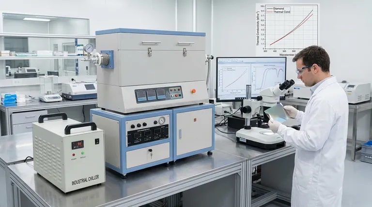
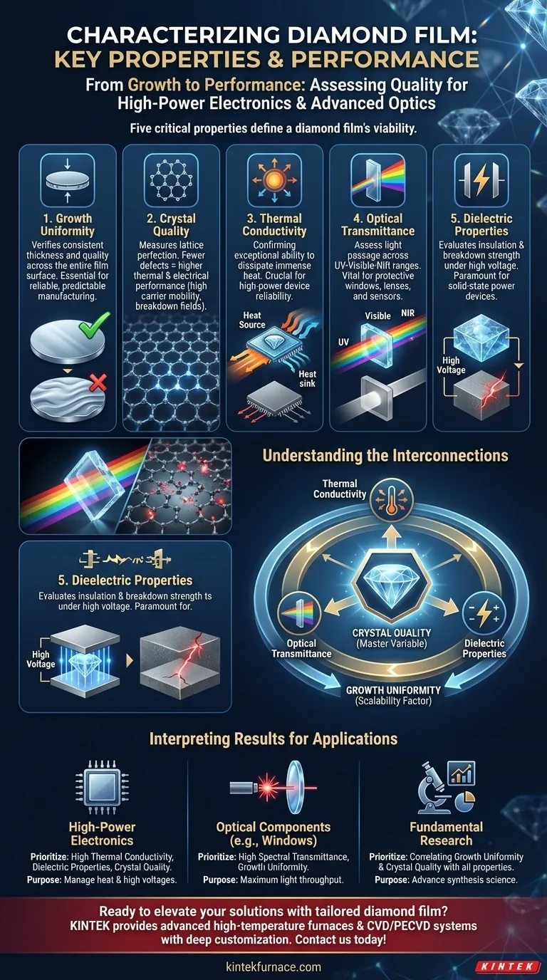
To assess its quality and application potential, the diamond film was characterized for a specific set of key properties. These included its growth uniformity, the crystal quality at various positions, its thermal conductivity at room temperature, its spectral transmittance across the UV-Visible-NIR range, and its dielectric properties.
The specific properties chosen for characterization are not arbitrary. They are a direct evaluation of the film's viability for demanding applications in high-power electronics and advanced optics, where material perfection is non-negotiable.
Why These Properties Matter: From Growth to Performance
Characterizing a diamond film is a process of verifying its fundamental capabilities. Each test provides a critical piece of data that determines its suitability for a specific, high-performance role.
Verifying Growth Uniformity
For any material to be useful in manufacturing, its properties must be consistent across its entire surface.
Measuring growth uniformity confirms that the film's thickness and quality do not vary from one point to another. Non-uniformity leads to unpredictable performance and device failure, making it a critical first check.
Assessing Crystal Quality
Diamond's exceptional properties are a direct result of its perfectly ordered carbon atom lattice.
"Crystal quality" is a measure of this perfection. Defects, impurities, or misaligned atoms in the crystal structure degrade its performance, particularly its electrical and thermal capabilities. High crystal quality is a prerequisite for achieving the high carrier mobility and breakdown fields that make diamond the "ultimate semiconductor."
Measuring Thermal Conductivity
High-power electronic devices generate immense heat. The ability to dissipate this heat is often the primary factor limiting performance and reliability.
Diamond possesses the highest thermal conductivity of any bulk material. Measuring this property confirms the film's ability to efficiently pull heat away from active components, preventing overheating and enabling operation at higher power levels.
Characterizing Optical Transmittance
This measurement determines how much light can pass through the diamond film at different wavelengths, from ultraviolet (UV) to near-infrared (NIR).
A high, uniform transmittance is essential for optical applications. This includes protective windows for high-power lasers, lenses for harsh environments, or transparent substrates for sensors where maximum light throughput is required.
Evaluating Dielectric Properties
Dielectric properties define how a material behaves in an electric field, specifically its ability to act as an insulator and resist electrical breakdown under high voltage.
For solid-state power devices, a high breakdown field is paramount. Characterizing these properties verifies that the diamond film can withstand the extreme electrical stresses present in next-generation electronics without failing.
Understanding the Interconnections
No single property exists in isolation. The results of these characterizations are deeply interconnected, often pointing back to the quality of the material's synthesis.
Crystal Quality as the Master Variable
Poor crystal quality is the root cause of diminished performance across the board.
A film with numerous defects will exhibit lower thermal conductivity because the lattice imperfections scatter heat-carrying vibrations. Similarly, these defects can absorb or scatter light, reducing optical transmittance, and create weak points that lower the material's dielectric strength.
Uniformity as the Scalability Factor
Even a small, perfect diamond crystal has limited use if the quality cannot be replicated over a larger area.
Ensuring uniformity is key to making diamond technology manufacturable and cost-effective. It proves that the high-quality properties measured in one spot are present across the entire wafer, enabling the production of multiple reliable devices.
Interpreting the Characterization Results
The significance of these characterization results depends entirely on the intended application of the diamond film.
- If your primary focus is high-power electronics: You must prioritize high thermal conductivity, excellent dielectric properties, and superior crystal quality to manage heat and high voltages.
- If your primary focus is optical components (e.g., windows): The most critical metric is high spectral transmittance across the required wavelength range, coupled with good surface uniformity.
- If your primary focus is fundamental materials research: The goal is to correlate growth uniformity and crystal quality with all other measured properties to advance the science of diamond synthesis.
Ultimately, a comprehensive characterization provides the essential blueprint for transitioning a promising material into a reliable technology.
Summary Table:
| Property | Purpose |
|---|---|
| Growth Uniformity | Ensures consistent thickness and quality across the film for reliable manufacturing. |
| Crystal Quality | Measures lattice perfection for high carrier mobility and breakdown fields in electronics. |
| Thermal Conductivity | Confirms heat dissipation capability for high-power device reliability. |
| Optical Transmittance | Assesses light passage across UV-Visible-NIR range for optical applications. |
| Dielectric Properties | Evaluates insulation and breakdown strength under high voltage for electronics. |
Ready to elevate your high-power electronics or advanced optics with tailored diamond film solutions? KINTEK leverages exceptional R&D and in-house manufacturing to provide advanced high-temperature furnace systems like Muffle, Tube, Rotary Furnaces, Vacuum & Atmosphere Furnaces, and CVD/PECVD Systems. Our deep customization capabilities ensure precise alignment with your unique experimental needs, helping you achieve superior material performance. Contact us today to discuss how we can support your innovation!
Visual Guide
Related Products
- HFCVD Machine System Equipment for Drawing Die Nano Diamond Coating
- 915MHz MPCVD Diamond Machine Microwave Plasma Chemical Vapor Deposition System Reactor
People Also Ask
- What are the equipment for chemical vapor deposition? A Guide to the 5 Essential Components
- What materials are commonly used in CVD coating systems? Explore Key Materials for Superior Coatings
- What role does Chemical Vapor Deposition (CVD) equipment play in the surface coating of carbon fibers for composites?
- How can customers maximize the quality of CVD coatings? Master Pre-Coating Prep for Superior Results
- What is the function of high-purity Argon (Ar) gas during CVD? Optimize Your Thin Film Uniformity and Purity

