At its core, the primary practical application of gate media prepared by CVD tube furnaces is in the manufacturing of advanced MOSFETs (Metal-Oxide-Semiconductor Field-Effect Transistors). These transistors are the fundamental building blocks of virtually all modern digital electronics, including computer processors and memory chips.
The question isn't just about one specific application, but about a foundational manufacturing capability. Chemical Vapor Deposition (CVD) in a tube furnace is a high-precision technique for depositing atomically thin, ultra-pure films, a requirement that extends far beyond just one component in electronics.
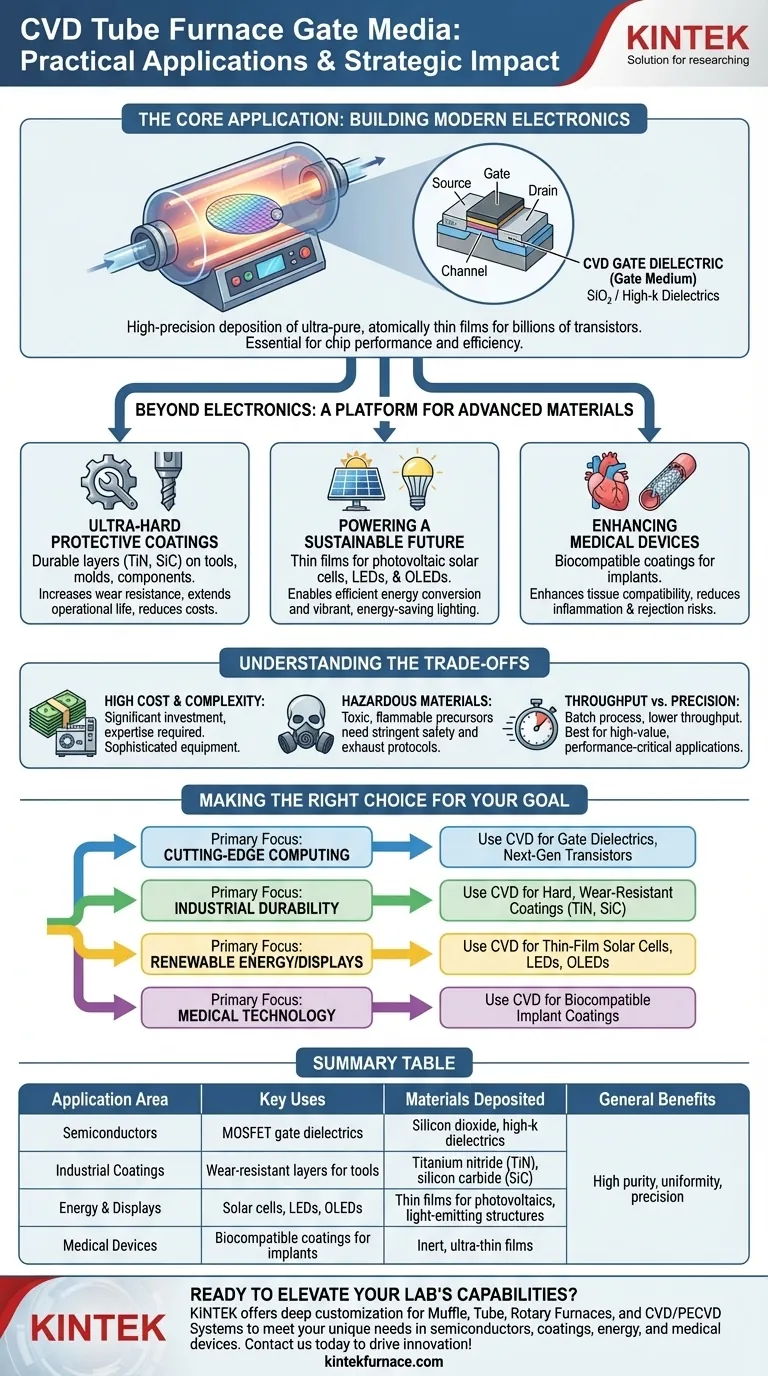
The Core Application: Building Modern Electronics
The most critical and high-volume application for gate media produced via CVD is in the semiconductor industry. This process is fundamental to creating the microscopic switches that power our digital world.
What is Gate Media?
In a transistor (MOSFET), the "gate" acts as a switch that controls the flow of electrical current. The gate medium, or more commonly the gate dielectric, is an ultrathin insulating layer that separates the gate from the current-carrying channel.
Its quality determines the transistor's performance and efficiency. Flaws in this layer, even at an atomic scale, can render a chip useless.
Why CVD is Essential for Transistors
CVD is the preferred method for depositing these films because it offers unparalleled control over thickness, purity, and uniformity. This precision is non-negotiable when manufacturing chips with billions of transistors.
The process allows for the deposition of critical materials like silicon dioxide and more advanced high-k dielectrics, which are necessary to prevent current leakage in smaller, more powerful transistors.
Beyond Electronics: A Platform for Advanced Materials
While semiconductor manufacturing is the primary driver, the capabilities of CVD tube furnaces extend to many other high-technology fields that require high-performance thin films.
Creating Ultra-Hard Protective Coatings
CVD can apply exceptionally durable layers of materials like titanium nitride (TiN) and silicon carbide (SiC) onto industrial tools, molds, and mechanical components.
These coatings dramatically increase wear resistance and extend the operational life of the underlying part, improving efficiency and reducing costs in manufacturing environments.
Powering a Sustainable Future
The technology is crucial in the energy and display sectors. It is used to produce the thin films required for photovoltaic solar cells, converting sunlight into electricity more efficiently.
Similarly, CVD is used in the fabrication of LEDs and OLEDs, depositing the precise layers of material needed to generate light for energy-efficient lighting and vibrant displays.
Enhancing Medical Devices
In the biomedical field, CVD furnaces are used to apply biocompatible coatings to medical implants like heart valves and vascular stents.
These inert, ultra-thin films enhance the device's compatibility with human tissue, significantly reducing the risk of inflammation, rejection, and blood clots.
Understanding the Trade-offs
While powerful, the CVD process is not a universal solution. It involves specific challenges and limitations that define its ideal use cases.
High Cost and Complexity
CVD furnace systems are sophisticated and expensive pieces of equipment. Operating them effectively requires significant technical expertise and investment in infrastructure, particularly for handling the precursor chemicals.
Hazardous Materials
The precursor gases used in the CVD process are often toxic, flammable, or corrosive. This necessitates stringent safety protocols, specialized handling equipment, and robust exhaust management systems, adding to the operational complexity.
Throughput vs. Precision
CVD in a tube furnace is typically a batch process. While it delivers exceptional film quality and precision, its throughput can be lower than other deposition techniques. This makes it best suited for high-value applications where material performance is more critical than raw production speed.
Making the Right Choice for Your Goal
The value of CVD is best understood by aligning its capabilities with a specific technological objective.
- If your primary focus is cutting-edge computing: CVD is the essential tool for depositing the gate dielectrics and other critical thin films required for next-generation transistors.
- If your primary focus is industrial durability: Use CVD to apply hard, wear-resistant coatings like TiN or SiC to extend the life of tools and high-performance components.
- If your primary focus is renewable energy or displays: This process is key for fabricating the active layers in thin-film solar cells and the light-emitting structures in LEDs and OLEDs.
- If your primary focus is medical technology: Apply CVD to develop biocompatible coatings that improve the safety and longevity of implantable medical devices.
Ultimately, the CVD tube furnace is a foundational tool for translating materials science breakthroughs into tangible technological advancements.
Summary Table:
| Application Area | Key Uses | Materials Deposited |
|---|---|---|
| Semiconductors | MOSFET gate dielectrics, transistors | Silicon dioxide, high-k dielectrics |
| Industrial Coatings | Wear-resistant layers for tools | Titanium nitride (TiN), silicon carbide (SiC) |
| Energy & Displays | Solar cells, LEDs, OLEDs | Thin films for photovoltaics, light-emitting structures |
| Medical Devices | Biocompatible coatings for implants | Inert, ultra-thin films |
| General Benefits | High purity, uniformity, precision | Various advanced materials |
Ready to elevate your lab's capabilities with custom high-temperature furnace solutions? At KINTEK, we leverage exceptional R&D and in-house manufacturing to provide advanced solutions like Muffle, Tube, Rotary Furnaces, Vacuum & Atmosphere Furnaces, and CVD/PECVD Systems. Our strong deep customization capability ensures we precisely meet your unique experimental needs, whether you're developing semiconductors, durable coatings, energy devices, or medical implants. Contact us today to discuss how our tailored furnace technologies can drive your innovations forward!
Visual Guide
Related Products
- Custom Made Versatile CVD Tube Furnace Chemical Vapor Deposition CVD Equipment Machine
- Split Chamber CVD Tube Furnace with Vacuum Station CVD Machine
- Multi Heating Zones CVD Tube Furnace Machine for Chemical Vapor Deposition Equipment
- Slide PECVD Tube Furnace with Liquid Gasifier PECVD Machine
- Inclined Rotary Plasma Enhanced Chemical Deposition PECVD Tube Furnace Machine
People Also Ask
- Why are CVD tube furnace sintering systems indispensable for 2D material research and production? Unlock Atomic-Scale Precision
- How might AI and machine learning enhance CVD tube furnace processes? Boost Quality, Speed, and Safety
- What temperature range do standard CVD tube furnaces operate at? Unlock Precision for Your Material Deposition
- Which industries and research fields benefit from CVD tube furnace sintering systems for 2D materials? Unlock Next-Gen Tech Innovations
- What customization options are available for CVD tube furnaces? Tailor Your System for Superior Material Synthesis