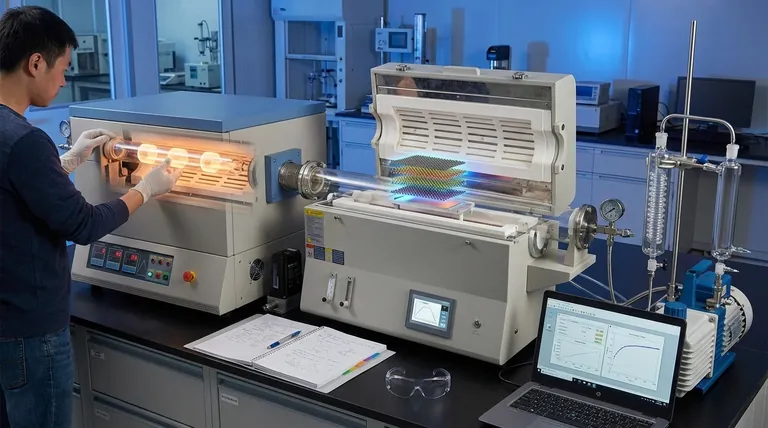
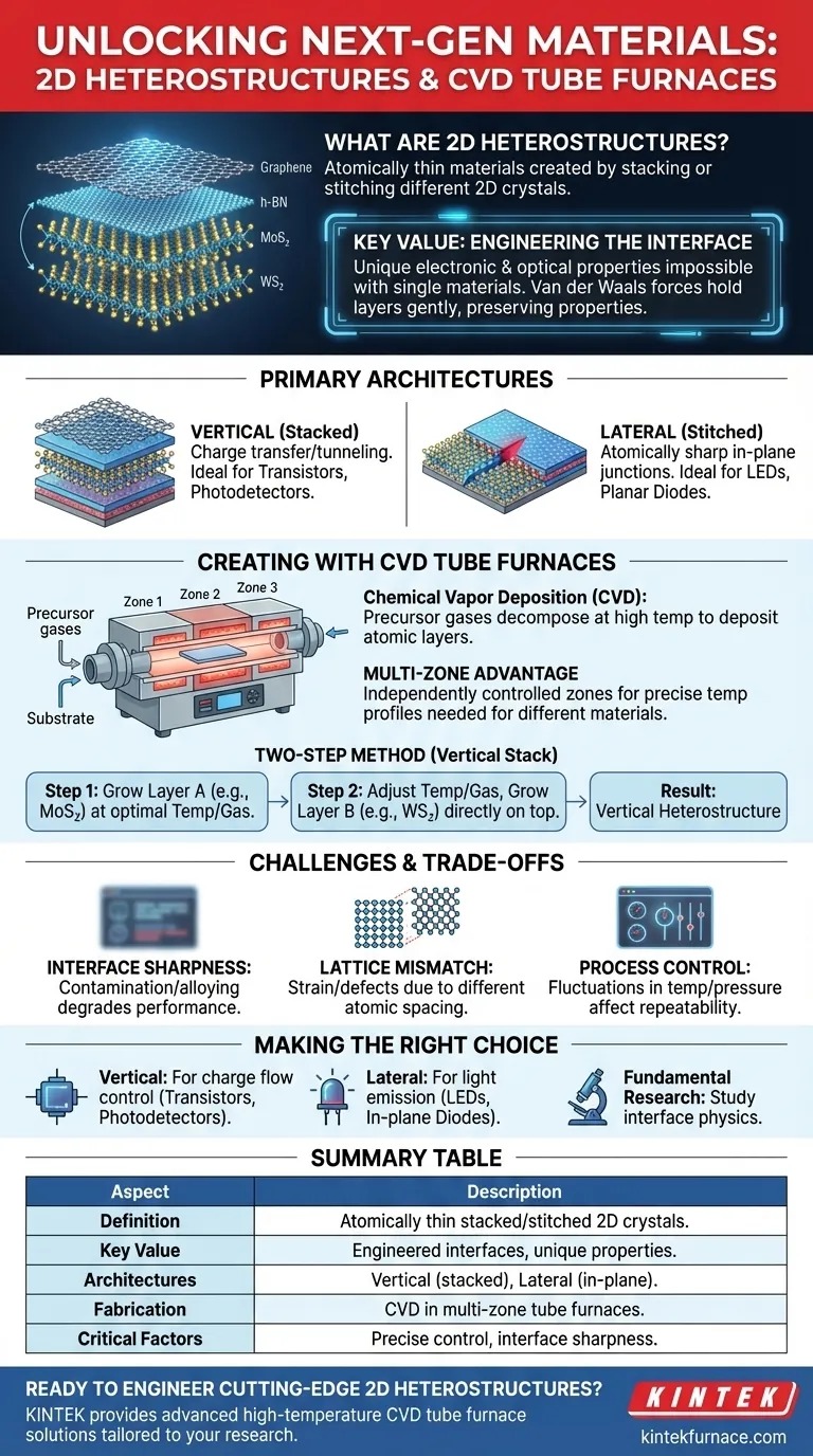
At their core, 2D heterostructures are atomically thin materials created by stacking or stitching together different two-dimensional crystals, such as graphene and hexagonal boron nitride (h-BN) or MoS₂ and WS₂. These structures are fabricated using a high-precision process called Chemical Vapor Deposition (CVD) inside specialized multi-zone tube furnaces, which enables the controlled, layer-by-layer growth required to build them.
The fundamental value of 2D heterostructures is not just in stacking thin materials, but in engineering the interface between them. This atomic-scale engineering creates unique electronic and optical properties that are impossible to achieve with any single material alone.
The Principle of 2D Heterostructures
Beyond a Simple Stack
Think of 2D heterostructures less as a simple sandwich and more as an atomically precise assembly. The interface where two different 2D materials meet is not just a boundary; it's a functional region where charge carriers, light, and energy interact in novel ways.
This controlled interaction is the key to designing next-generation transistors, photodetectors, and quantum computing components.
The Role of van der Waals Forces
The individual layers in a stacked heterostructure are held together by weak van der Waals forces. This is crucial because it allows the layers to interact electronically and optically without disrupting the fundamental crystal structure of each individual material.
This "gentle" bonding preserves the unique properties of each layer while enabling the creation of a new, combined system.
Vertical vs. Lateral Architectures
There are two primary configurations for 2D heterostructures, each built for a different purpose.
Vertical heterostructures involve stacking one material directly on top of another, like layers of a cake. This is ideal for devices that rely on charge transfer or tunneling between layers.
Lateral heterostructures involve stitching two materials together side-by-side in the same plane, like a quilt. This creates an atomically sharp, in-plane junction, perfect for devices like light-emitting diodes (LEDs) or specialized planar transistors.
Creating Heterostructures with CVD Tube Furnaces
The CVD Process Explained
Chemical Vapor Deposition (CVD) is the cornerstone technique for creating high-quality 2D materials. In this process, precursor gases containing the required elements are introduced into a high-temperature vacuum tube.
The heat causes the gases to decompose and react, depositing a single, uniform atomic layer of the desired material onto a substrate.
Why Multi-Zone Furnaces Are Critical
A standard furnace has one temperature zone. However, different 2D materials grow at different optimal temperatures and require different precursor gases.
Multi-zone tube furnaces are the enabling technology here. They have several independently controlled heating zones, allowing a researcher to create a precise temperature profile along the length of the tube to grow one material after another.
The Two-Step Method for Vertical Stacks
To create a vertical stack like MoS₂/WS₂, a two-step CVD process is used.
First, the furnace is set to the optimal temperature for MoS₂ growth, and its precursors are introduced to grow the first layer. Once complete, the gas mixture is switched to the precursors for WS₂, and the temperature profile is adjusted to grow the second layer directly on top of the first, all within the same sealed environment.
Understanding the Trade-offs and Challenges
Achieving Atomically Sharp Interfaces
The ideal heterostructure has a perfectly clean and abrupt interface between materials. In reality, achieving this is a significant challenge.
Contamination between growth steps or unintended alloying at the boundary can degrade the device's electronic or optical performance.
The Problem of Lattice Mismatch
Every crystal has a specific atomic spacing, known as its lattice constant. When stacking two materials with different lattice constants, the mismatch can introduce strain, wrinkles, or defects into the layers.
This strain can sometimes be used advantageously, but it can also negatively impact device reliability and performance.
Process Control and Repeatability
Synthesizing the exact same high-quality heterostructure from one experiment to the next is notoriously difficult. Minor fluctuations in temperature, pressure, or gas flow can lead to variations in quality.
This challenge is a major hurdle for moving 2D heterostructure devices from the laboratory to industrial-scale manufacturing.
Making the Right Choice for Your Goal
The architecture you choose depends entirely on the device function you aim to achieve.
- If your primary focus is building transistors or photodetectors: Vertical heterostructures are the ideal choice, as they allow you to control charge flow and separation between distinct material layers.
- If your primary focus is creating in-plane diodes or LEDs: Lateral heterostructures provide the seamless, atomically sharp p-n junctions needed for efficient light emission and in-plane electronics.
- If your primary focus is fundamental materials research: The two-step CVD process in a multi-zone furnace gives you the control needed to study the physics of the interface itself, which is often the most scientifically interesting part.
Mastering this fabrication process is the key to engineering materials at the atomic level, unlocking the next generation of electronic and quantum devices.
Summary Table:
| Aspect | Description |
|---|---|
| Definition | Atomically thin materials stacked or stitched from 2D crystals like graphene, h-BN, MoS₂, WS₂ |
| Key Value | Engineered interfaces enable unique electronic, optical properties not possible with single materials |
| Primary Architectures | Vertical (stacked layers) for transistors, photodetectors; Lateral (in-plane junctions) for LEDs, diodes |
| Fabrication Method | Chemical Vapor Deposition (CVD) in multi-zone tube furnaces for layer-by-layer growth |
| Critical Factors | Precise temperature control, gas flow, and interface sharpness to avoid defects and ensure repeatability |
Ready to engineer cutting-edge 2D heterostructures for your research or devices? Leveraging exceptional R&D and in-house manufacturing, KINTEK provides diverse laboratories with advanced high-temperature furnace solutions. Our product line, including Muffle, Tube, Rotary Furnaces, Vacuum & Atmosphere Furnaces, and CVD/PECVD Systems, is complemented by our strong deep customization capability to precisely meet unique experimental requirements. Contact us today to discuss how our tailored CVD tube furnaces can enhance your material synthesis and drive innovation in electronics, optics, and quantum technologies!
Visual Guide
Related Products
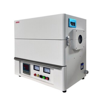
- Custom Made Versatile CVD Tube Furnace Chemical Vapor Deposition CVD Equipment Machine
- Split Chamber CVD Tube Furnace with Vacuum Station CVD Machine
- Multi Heating Zones CVD Tube Furnace Machine for Chemical Vapor Deposition Equipment
- Slide PECVD Tube Furnace with Liquid Gasifier PECVD Machine
- Inclined Rotary Plasma Enhanced Chemical Deposition PECVD Tube Furnace Machine
People Also Ask
- What is a CVD tube furnace and what is its primary function? Discover Precision Thin-Film Deposition
- What are the benefits of developing new precursor materials for CVD tube furnaces? Unlock Advanced Thin-Film Synthesis
- What customization options are available for CVD tube furnaces? Tailor Your System for Superior Material Synthesis
- What temperature range do standard CVD tube furnaces operate at? Unlock Precision for Your Material Deposition
- Why are CVD tube furnace sintering systems indispensable for 2D material research and production? Unlock Atomic-Scale Precision