At its core, Chemical Vapor Deposition (CVD) is a uniquely versatile materials synthesis process. It is used to create a vast range of high-purity thin films and coatings, including critical electronic materials like silicon, pure metals like tungsten, advanced ceramics such as carbides and nitrides, and revolutionary carbon structures like graphene and synthetic diamond.
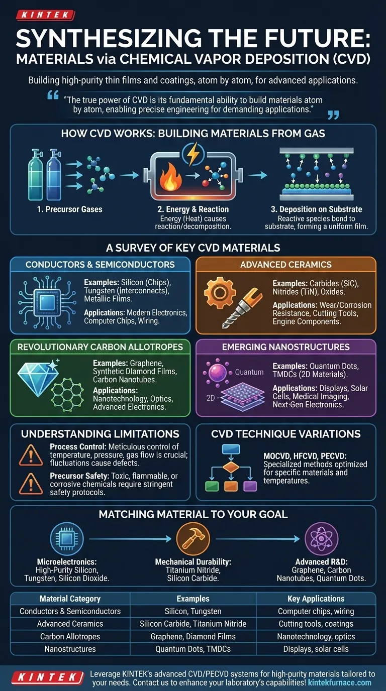
The true power of CVD is not just the wide variety of materials it can produce, but its fundamental ability to build these materials atom by atom. By controlling chemical reactions in a gas phase, CVD enables the precise engineering of thin films with exceptional purity and performance for highly demanding applications.
How CVD Works: Building Materials from Gas
The Core Principle
Chemical Vapor Deposition is a "bottom-up" manufacturing technique. The process begins by introducing volatile precursor gases, which contain the atoms of the desired material, into a reaction chamber.
The Role of Energy and Reaction
Energy, typically in the form of high heat, is applied to the chamber. This energy causes the precursor gases to react or decompose, breaking them down into their constituent elements or new chemical species.
Deposition onto a Substrate
These newly formed, reactive species then travel to the surface of a target object, known as the substrate. They bond to this surface and gradually build up, layer by layer, to form a solid, uniform thin film or coating. Precise control over temperature, pressure, and gas flow is critical to achieving the desired material properties.
A Survey of Key CVD Materials
Conductors and Semiconductors
CVD is the backbone of the modern electronics industry. It is used to deposit the ultrapure silicon that forms the basis of computer chips, as well as the metallic films (like tungsten) that create the intricate wiring connecting billions of transistors.
Advanced Ceramics and Compounds
This category includes extremely hard and resilient materials. Carbides (e.g., silicon carbide), nitrides (e.g., titanium nitride), and oxides are deposited as protective coatings on cutting tools, engine components, and other parts to dramatically increase wear and corrosion resistance.
Revolutionary Carbon Allotropes
CVD is instrumental in synthesizing some of the most advanced materials known. This includes graphene (a single layer of carbon atoms with remarkable electronic properties), synthetic diamond films (for superior cutting tools and optical windows), and carbon nanotubes (for nanotechnology and advanced electronics).
Emerging Nanostructures
The precision of CVD allows for the creation of sophisticated nanostructures. This includes quantum dots, which are semiconductor nanocrystals used in advanced displays, solar cells, and medical imaging, as well as Transition Metal Dichalcogenides (TMDCs), which are 2D materials with significant potential for next-generation electronics.
Understanding the Process Limitations
The Challenge of Process Control
The quality and properties of a CVD-deposited film are directly dependent on meticulous control of the process variables. Even small fluctuations in temperature, pressure, or gas flow can lead to defects, impurities, and inconsistent results.
Precursor Selection and Safety
Choosing the correct precursor chemicals is a complex task. These chemicals must be volatile enough to exist as a gas but stable enough to be handled. Many precursors are also toxic, flammable, or corrosive, requiring stringent safety protocols and specialized handling equipment.
Variations of the CVD Technique
There is no single "CVD" process. The technique has numerous specialized variations designed to optimize for specific materials or overcome challenges. Methods like Metalorganic CVD (MOCVD), Hot-Filament CVD (HFCVD), and Plasma-Enhanced CVD (PECVD) are tailored for different temperature sensitivities and material outcomes.
Matching the Material to Your Goal
Selecting the right CVD material requires aligning its unique properties with your specific industrial or research objective.
- If your primary focus is microelectronics: Your key materials are high-purity silicon for transistors, tungsten for conductive interconnects, and silicon dioxide for insulation.
- If your primary focus is mechanical durability: You should consider ceramic coatings like titanium nitride and silicon carbide for superior hardness and wear resistance on tools and parts.
- If your primary focus is advanced research and development: Your interest lies with materials like graphene, carbon nanotubes, and quantum dots for their novel electronic, optical, and structural properties.
Ultimately, the power of CVD lies in its ability to engineer materials from the atoms up, opening a vast landscape of technological possibilities.
Summary Table:
| Material Category | Examples | Key Applications |
|---|---|---|
| Conductors & Semiconductors | Silicon, Tungsten | Computer chips, electronic wiring |
| Advanced Ceramics | Silicon Carbide, Titanium Nitride | Cutting tools, wear-resistant coatings |
| Carbon Allotropes | Graphene, Diamond Films | Nanotechnology, optics, electronics |
| Nanostructures | Quantum Dots, TMDCs | Displays, solar cells, medical imaging |
Leverage KINTEK's advanced CVD/PECVD systems and deep customization capabilities to synthesize high-purity materials tailored to your unique needs. Whether you're in electronics, materials science, or R&D, our solutions deliver precision and performance. Contact us today to discuss how we can enhance your laboratory's capabilities!
Visual Guide
Related Products
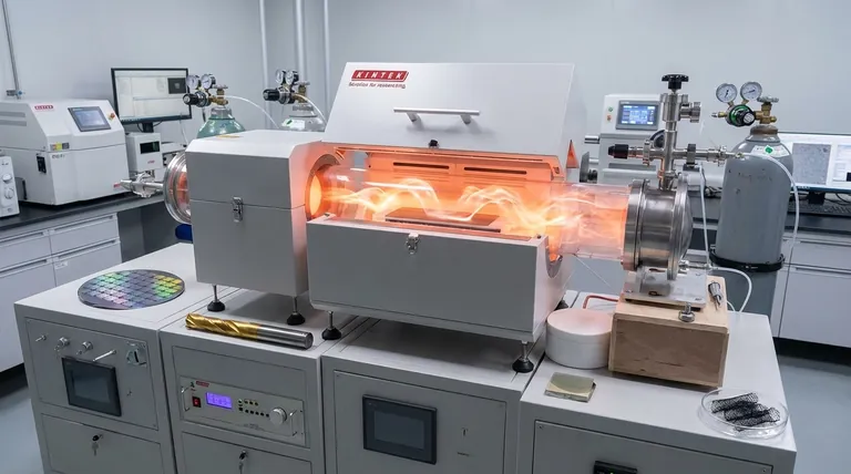
- Custom Made Versatile CVD Tube Furnace Chemical Vapor Deposition CVD Equipment Machine
- Split Chamber CVD Tube Furnace with Vacuum Station CVD Machine
- Multi Heating Zones CVD Tube Furnace Machine for Chemical Vapor Deposition Equipment
- Slide PECVD Tube Furnace with Liquid Gasifier PECVD Machine
- Controlled Inert Nitrogen Hydrogen Atmosphere Furnace
People Also Ask
- What are the key application fields of CVD tube furnaces? Unlock Precision in Thin-Film Synthesis
- What improvements can be made to the bonding force of gate dielectric films using a CVD tube furnace? Enhance Adhesion for Reliable Devices
- What is the working principle of a CVD tube furnace? Achieve Precise Thin Film Deposition for Your Lab
- Which industries and research fields benefit from CVD tube furnace sintering systems for 2D materials? Unlock Next-Gen Tech Innovations
- How does CVD tube furnace sintering enhance graphene growth? Achieve Superior Crystallinity and High Electron Mobility


