In short, chemical vapor deposition (CVD) is a highly versatile method used to create an entire family of advanced carbon-based materials. These range from exceptionally hard diamond films to revolutionary nanomaterials like graphene and carbon nanotubes, all by precisely controlling how carbon atoms are assembled on a surface.
The true power of CVD lies in its ability to manipulate the atomic structure of carbon. By tuning the process, you can create materials with vastly different properties—from the ultimate hardness of diamond to the unique electronic capabilities of graphene—all from the same fundamental element.
Understanding the Spectrum of CVD Diamond Films
The term "diamond film" isn't monolithic. The key differentiator is the crystalline structure, which dictates the material's performance and cost. CVD allows for precise control over this structure.
Single-Crystal Diamond (SCD)
Think of single-crystal diamond as a flawless, continuous lattice of carbon atoms. It represents the highest possible quality of diamond.
Because it lacks grain boundaries or defects, SCD exhibits the most extreme and uniform properties: the highest thermal conductivity, hardness, and charge carrier mobility. This makes it the gold standard for high-performance optics, quantum sensing, and advanced electronics.
Polycrystalline Diamond (PCD)
Polycrystalline diamond is composed of many small, individual diamond crystals (grains) that are fused together. Imagine it as a tightly packed mosaic of microscopic diamonds.
While the grain boundaries slightly reduce its overall performance compared to SCD, PCD is far easier and more cost-effective to produce over large areas. This makes it ideal for durable coatings on cutting tools, wear-resistant surfaces, and thermal management components where large-area coverage is essential. The films can be grown as thin layers or as thick, self-supporting wafers.
Exploring Other Carbon Nanostructures
Beyond the classic diamond lattice, CVD can create other arrangements of carbon atoms, known as allotropes, each with unique dimensionality and game-changing properties.
Graphene: The 2D Revolution
Graphene is a single, flat sheet of carbon atoms arranged in a honeycomb pattern. It is the world's thinnest, strongest, and most conductive material.
Its two-dimensional nature and incredible electronic properties make it a candidate for next-generation transparent electrodes, ultra-fast transistors, and highly sensitive biosensors.
Carbon Nanotubes (CNTs): The 1D Powerhouse
Carbon nanotubes are essentially sheets of graphene rolled up into seamless cylinders. These one-dimensional structures are exceptionally strong and have unique electrical properties that depend on how they are rolled.
They are being explored for use in reinforcing composite materials, creating tiny electrical interconnects in microchips, and as components in advanced sensors and energy storage devices.
Fullerenes: The Molecular Spheres
Fullerenes are molecules of carbon arranged in a hollow sphere, ellipsoid, or tube. The most famous is the C60 molecule, or "buckyball," which resembles a soccer ball.
While less common for film deposition, CVD processes can be adapted to produce these nanostructures, which have applications in medicine, lubricants, and photovoltaics.
Understanding the Trade-offs: Structure vs. Application
Choosing the right CVD carbon material requires understanding the inherent trade-offs between ideal properties and practical constraints.
Purity vs. Scalability
Single-crystal diamond offers theoretical perfection but is difficult and expensive to grow, especially over large areas.
Polycrystalline diamond sacrifices some of that perfection for scalability. It delivers excellent diamond-like properties over large, complex surfaces at a much lower cost, making it the practical choice for most industrial coating applications.
Dimensionality and Properties
The dimensionality of the material profoundly impacts its use. Graphene's 2D nature is perfect for transparent, flexible electronics. The 1D structure of CNTs provides incredible strength along their length, ideal for reinforcement. Diamond's 3D lattice provides isotropic hardness and thermal conductivity, perfect for robust optics and heat sinks.
Making the Right Choice for Your Goal
Your application's primary requirement will guide your material selection.
- If your primary focus is ultimate performance and purity: Single-crystal diamond is the only choice for applications like high-power electronics or quantum computing.
- If your primary focus is durable, large-area coatings: Polycrystalline diamond films offer the best balance of performance, cost, and scalability for tools and thermal management.
- If your primary focus is next-generation flexible electronics: Graphene's unique combination of transparency, conductivity, and strength is unmatched.
- If your primary focus is high-strength composites or nanoscale wiring: Carbon nanotubes provide exceptional tensile strength and electrical conductivity in a lightweight form factor.
Ultimately, CVD provides a complete toolbox for engineering carbon, allowing you to select the precise material structure that best solves your specific technical challenge.
Summary Table:
| Material Type | Key Characteristics | Common Applications |
|---|---|---|
| Single-Crystal Diamond (SCD) | Highest purity, thermal conductivity & hardness; flawless lattice | High-performance optics, quantum sensing, advanced electronics |
| Polycrystalline Diamond (PCD) | Cost-effective, scalable, durable; composed of fused micro-crystals | Cutting tools, wear-resistant coatings, thermal management |
| Graphene (2D) | World's thinnest & strongest material; highly conductive & transparent | Flexible electronics, transparent electrodes, biosensors |
| Carbon Nanotubes (1D) | Exceptional strength; tunable electrical properties | Composite materials, nano-electronics, energy storage |
| Fullerenes | Hollow carbon molecules (e.g., C60 "buckyballs") | Medicine, photovoltaics, lubricants |
Unlock the Potential of Advanced Carbon Nanofilms with KINTEK
Navigating the spectrum of CVD carbon materials—from ultra-hard diamond films to conductive graphene—requires not just expertise, but the right equipment tailored to your specific research or production goals.
At KINTEK, we combine exceptional R&D with in-house manufacturing to provide diverse laboratories with advanced high-temperature furnace solutions. Our product line, including Muffle Furnaces, Tube Furnaces, Rotary Furnaces, Vacuum & Atmosphere Furnaces, and CVD/PECVD Systems, is engineered to support the precise synthesis of SCD, PCD, graphene, CNTs, and other carbon nanostructures.
What sets us apart is our strong deep customization capability. Whether you need to scale up polycrystalline diamond coatings or experiment with novel graphene applications, we work with you to modify or design a system that precisely meets your unique experimental requirements.
Ready to engineer the future with carbon? Let's discuss how our tailored solutions can accelerate your project.
Contact our experts today for a personalized consultation.
Visual Guide

Related Products
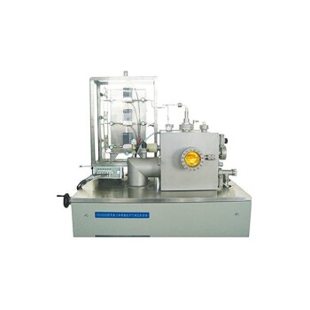
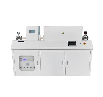
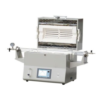
- Custom Made Versatile CVD Tube Furnace Chemical Vapor Deposition CVD Equipment Machine
- HFCVD Machine System Equipment for Drawing Die Nano Diamond Coating
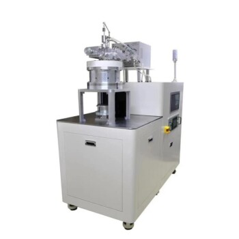
- RF PECVD System Radio Frequency Plasma Enhanced Chemical Vapor Deposition
- Inclined Rotary Plasma Enhanced Chemical Deposition PECVD Tube Furnace Machine
- Multi Heating Zones CVD Tube Furnace Machine for Chemical Vapor Deposition Equipment
People Also Ask
- Where is a CVD Tube Furnace commonly used? Essential for High-Tech Materials and Electronics
- Why are high-purity quartz boats used for graphene oxide reduction? Ensure Chemical Purity & Thermal Stability
- What is the function of injecting water in wood thermal modification? Unlock Superior Stability and Hydrophobicity
- What advantages does the Laser Chemical Vapor Deposition (LCVD) process offer? High Purity & Precision SiC Fibers
- Which industries and research fields benefit from CVD tube furnace sintering systems for 2D materials? Unlock Next-Gen Tech Innovations
