At its core, the role of Microwave Plasma Chemical Vapor Deposition (MPCVD) in optical applications is to grow exceptionally pure, single-crystal diamonds. These lab-grown diamonds serve as the raw material for next-generation optical components that demand a combination of flawless transparency, extreme durability, and a wide transmission spectrum from ultraviolet to infrared light.
MPCVD is not merely a manufacturing step; it is the enabling technology that unlocks the theoretical potential of diamond for practical, high-performance optical systems. It solves the challenge of creating a material with unmatched optical clarity that can also withstand extreme physical and thermal stress.
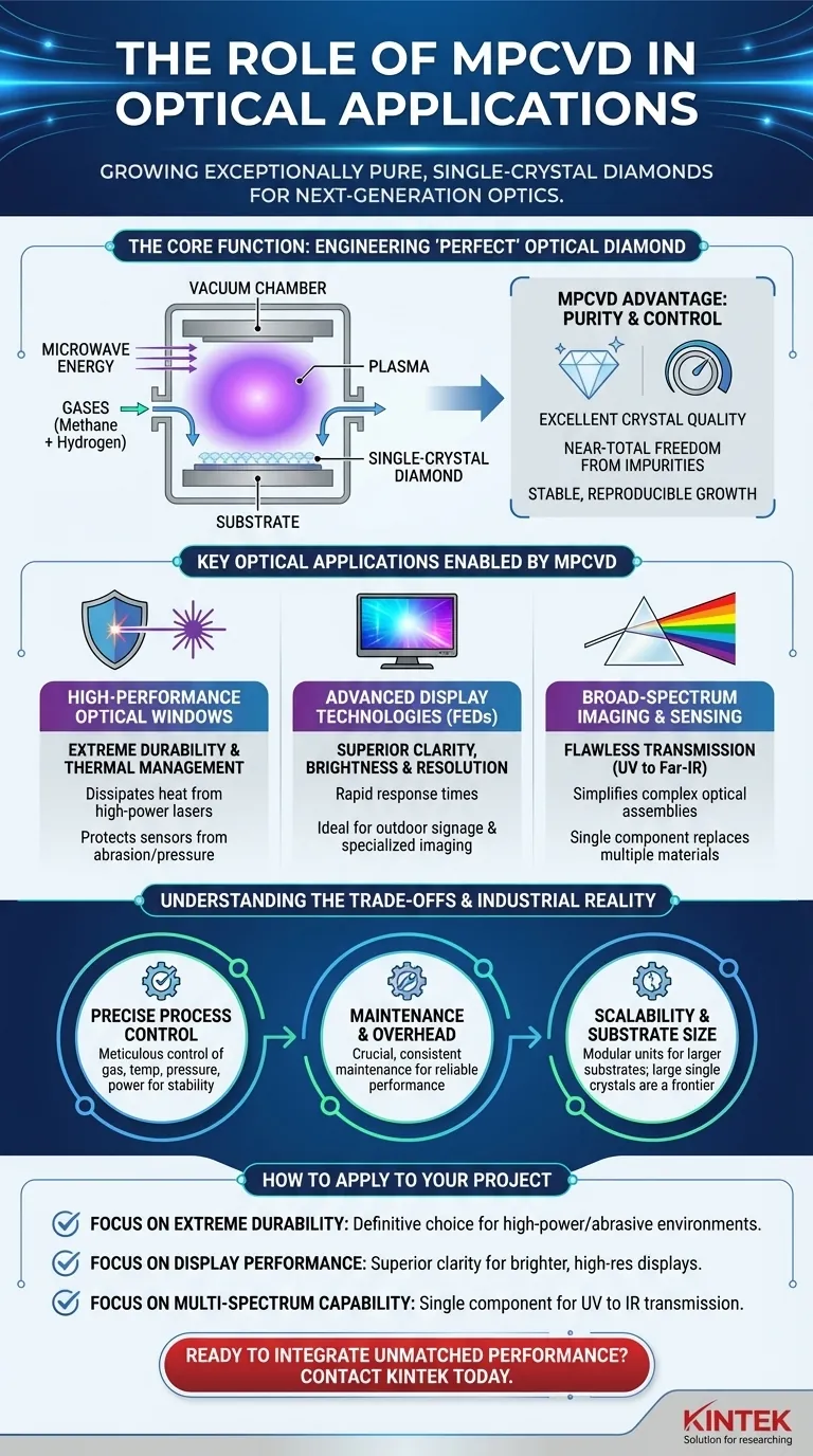
The Core Function: Engineering 'Perfect' Optical Diamond
To understand MPCVD's role, we must first understand why diamond is so desirable for optics and how MPCVD makes its use practical.
What is MPCVD?
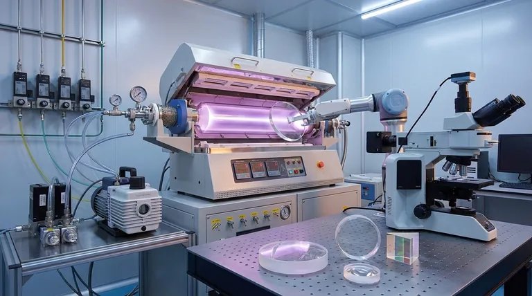
MPCVD stands for Microwave Plasma Chemical Vapor Deposition. It is an advanced process that uses microwave energy to create a plasma from a mixture of gases (typically methane and hydrogen). Inside a vacuum chamber, this plasma provides the conditions for carbon atoms to settle onto a substrate, layer by layer, forming a high-quality diamond crystal.
Why Diamond is the Ideal Optical Material
Natural diamond has long been recognized for its superb optical properties. Lab-grown diamond replicates and even improves upon these, offering a unique combination of benefits that no other material can match. Key properties include superior clarity and an extremely wide transmittance window.
The MPCVD Advantage: Purity and Control
The MPCVD process delivers excellent crystal quality with a near-total freedom from impurities. This level of process control is critical. Unlike other methods, MPCVD allows for the stable, reproducible growth of diamonds, which is essential for any industrial or high-stakes application.
Key Optical Applications Enabled by MPCVD
The ability to reliably produce this "perfect" material has unlocked several key applications where conventional optics fall short.
High-Performance Optical Windows
MPCVD-grown diamonds are used to create robust optical windows for devices operating in harsh environments. Their high thermal conductivity allows them to dissipate heat from high-power lasers, while their physical hardness protects sensitive sensors from abrasion and pressure.
Advanced Display Technologies
MPCVD diamond is a vital component in Cold Cathode Field Emission Displays (FEDs). The material's optical clarity results in displays with exceptional brightness, high resolution, and rapid response times. This is critical for outdoor signage and specialized, high-detail imaging systems.
Broad-Spectrum Imaging and Sensing
Because MPCVD diamond is transparent to a vast range of light, from deep ultraviolet (UV) to far-infrared (IR), a single diamond lens or window can replace multiple components made of different materials. This simplifies the design of scientific instruments and sensors that need to operate across multiple light spectrums.
Understanding the Trade-offs and Industrial Reality
While powerful, MPCVD technology is an industrial process with practical considerations that must be managed for successful implementation.
The Need for Precise Process Control
The exceptional quality of MPCVD diamond is not automatic. It depends on meticulous control over gas mixtures, temperature, pressure, and microwave power. Achieving stability and reproducibility requires significant process expertise.
Maintenance and Operational Overhead
As with any advanced deposition system, MPCVD equipment requires crucial and consistent maintenance. This ensures the equipment operates normally, extends its lifespan, and, most importantly, maintains the performance needed to produce high-purity crystals.
Scalability and Substrate Size
The technology is inherently scalable, often using modular units that allow for adaptation to larger substrates. However, growing very large, flawless single crystals remains a frontier of active development, which can be a limiting factor for certain large-format optics.
How to Apply This to Your Project
Your decision to specify or invest in MPCVD-diamond optics should be guided by the primary challenge you need to solve.
- If your primary focus is extreme durability: MPCVD diamond is the definitive choice for optical windows in high-power, high-pressure, or abrasive environments.
- If your primary focus is display performance: The superior clarity and properties of MPCVD diamond directly translate to brighter, higher-resolution displays that excel in demanding conditions.
- If your primary focus is multi-spectrum capability: A single MPCVD diamond component can provide flawless transmission from UV to IR, simplifying complex optical assemblies.
Ultimately, MPCVD empowers engineers and scientists to use the ideal optical material—diamond—without compromise.
Summary Table:
| Application | Key Benefit of MPCVD Diamond |
|---|---|
| Optical Windows | Extreme durability & thermal management for harsh environments |
| Advanced Displays (FEDs) | Superior clarity for high brightness & resolution |
| Broad-Spectrum Sensing | Flawless transmission from UV to IR, simplifying design |
Ready to integrate the unmatched performance of MPCVD diamond into your optical systems?
At KINTEK, we leverage exceptional R&D and in-house manufacturing to provide diverse laboratories with advanced high-temperature furnace solutions. Our product line, including CVD/PECVD Systems, is complemented by strong deep customization capability to precisely meet your unique experimental requirements for growing high-purity optical materials.
Contact our experts today to discuss how our MPCVD solutions can bring superior clarity, durability, and multi-spectrum capability to your project.
Visual Guide
Related Products
- 915MHz MPCVD Diamond Machine Microwave Plasma Chemical Vapor Deposition System Reactor
- Cylindrical Resonator MPCVD Machine System for Lab Diamond Growth
- MPCVD Machine System Reactor Bell-jar Resonator for Lab and Diamond Growth
- Multi Heating Zones CVD Tube Furnace Machine for Chemical Vapor Deposition Equipment
- HFCVD Machine System Equipment for Drawing Die Nano Diamond Coating
People Also Ask
- What are the main components of an MPCVD machine? Unlock the Secrets of Diamond Synthesis
- What is the basic principle of operation for the microwave plasma chemical vapor deposition system? Unlock High-Purity Material Growth
- What factors influence the quality of diamond deposition in the MPCVD method? Master the Critical Parameters for High-Quality Diamond Growth
- What are the essential components of an MPCVD reactor for diamond film deposition? Unlock High-Quality Diamond Growth
- What are some key features and benefits of the microwave plasma chemical vapor deposition system? Achieve Unmatched Material Synthesis


