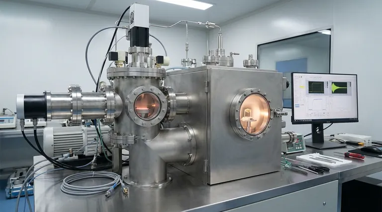
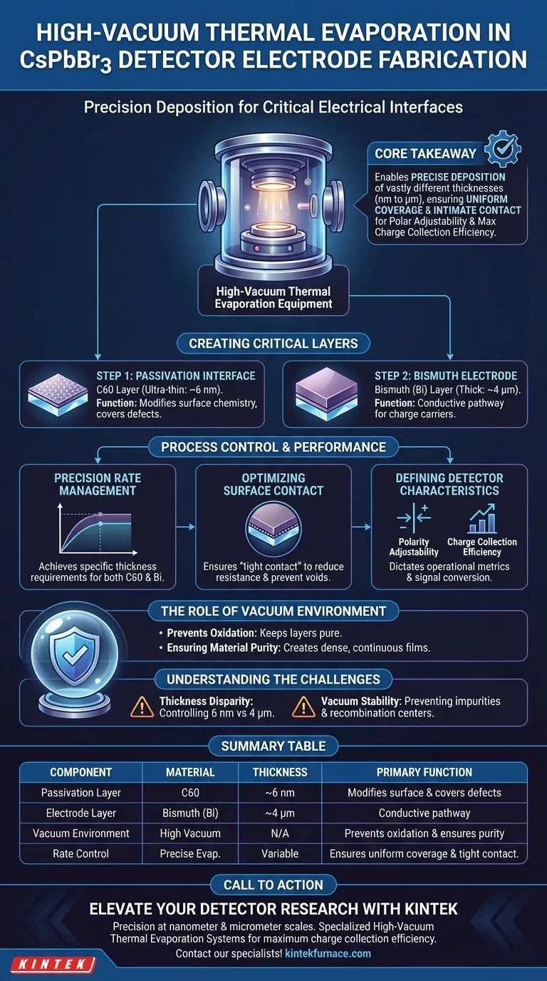
High-vacuum thermal evaporation equipment acts as the central fabrication tool for establishing the critical electrical interfaces on CsPbBr3 single crystal detectors. It is specifically responsible for sequentially depositing a 6 nm C60 passivation layer and a 4 micrometer Bismuth (Bi) electrode layer directly onto the crystal surface.
Core Takeaway The equipment’s primary value lies in its ability to deposit vastly different layer thicknesses—from nanometers to micrometers—with high precision. By managing evaporation rates in a controlled vacuum, it ensures the uniform coverage and intimate contact necessary to define the detector’s polarity adjustability and maximize charge collection efficiency.
Creating the Critical Functional Layers
The Passivation Interface
The initial role of the equipment is to deposit a C60 passivation layer.
This layer is extremely thin, measuring approximately 6 nanometers.
Its primary function is to modify the surface chemistry of the CsPbBr3 crystal before the bulk electrode is added.
The Bismuth Electrode
Following passivation, the equipment is used to deposit the main electrode material.
For this specific application, a Bismuth (Bi) layer is deposited to a thickness of approximately 4 micrometers.
This layer serves as the conductive pathway for charge carriers to exit the device.
Ensuring Device Performance through Process Control
Precision Rate Management
The equipment allows operators to strictly control the rate at which materials are evaporated.
This control is vital for achieving the specific thickness requirements of both the ultra-thin C60 layer and the much thicker Bi layer.
Optimizing Surface Contact
The performance of a radiation detector hinges on the quality of the interface between the crystal and the electrode.
Thermal evaporation ensures "tight contact" between the layers and the single crystal surface.
This physical intimacy reduces resistance and prevents voids that could trap charges.
Defining Detector Characteristics
The quality of these deposited layers directly dictates the operational metrics of the final device.
Specifically, the uniformity of the deposition determines the detector's polarity adjustability.
Furthermore, the integrity of the contact governs the charge collection efficiency, which is the measure of how effectively the detector converts radiation into an electrical signal.
The Role of the Vacuum Environment
Preventing Oxidation
While the primary focus is on deposition, the "high vacuum" aspect is functional, not just distinct.
Based on general principles of this technology, the vacuum environment prevents oxygen from interacting with the vaporized source materials.
This ensures that the deposited layers remain pure and free of oxides, which acts as insulators and degrades performance.
Ensuring Material Purity
The low-pressure environment allows vapor particles to travel to the substrate without colliding with gas molecules.
This creates a dense, continuous film rather than a porous or contaminated structure.
Understanding the Challenges
Thickness Disparity
A significant challenge in this process is managing the vast difference in scale between the two layers.
The equipment must be capable of finely controlling a 6 nm layer (C60) while also sustaining the deposition for a 4 $\mu$m layer (Bi).
Failure to switch gears effectively between these scales can lead to poor passivation or insufficient electrode conductivity.
Vacuum Stability
The quality of the film is entirely dependent on maintaining a stable vacuum.
Any fluctuation in pressure during the evaporation process can introduce impurities at the interface.
These impurities create recombination centers, which kill the electrical signal before it can be collected.
Optimizing Fabrication for Detector Quality
To maximize the performance of CsPbBr3 detectors, the evaporation process must be tailored to the specific function of each layer.
- If your primary focus is signal stability: Prioritize the precision of the C60 passivation layer deposition to ensure the crystal surface defects are adequately covered.
- If your primary focus is charge collection: Ensure the Bismuth deposition rate is optimized to create a dense, void-free bulk electrode that adheres tightly to the passivation layer.
The ultimate sensitivity of the detector is defined not just by the crystal quality, but by the integrity of the evaporated contacts that extract the signal.
Summary Table:
| Process Component | Material | Thickness | Primary Function |
|---|---|---|---|
| Passivation Layer | C60 | ~6 nm | Modifies surface chemistry & covers defects |
| Electrode Layer | Bismuth (Bi) | ~4 μm | Provides conductive pathway for charge carriers |
| Vacuum Environment | High Vacuum | N/A | Prevents oxidation & ensures high material purity |
| Rate Control | Precise Evaporation | Variable | Ensures uniform coverage & tight physical contact |
Elevate Your Single Crystal Detector Research with KINTEK
Precision at both the nanometer and micrometer scale is vital for high-performance electrode fabrication. Backed by expert R&D and manufacturing, KINTEK offers specialized High-Vacuum Thermal Evaporation systems, alongside our Muffle, Tube, Rotary, and CVD systems, all customizable for your unique lab requirements.
Whether you are depositing sensitive passivation layers or bulk metal electrodes, our equipment ensures the vacuum stability and rate control necessary for maximum charge collection efficiency.
Ready to optimize your thin-film deposition process?
Contact our specialists today to find the perfect solution for your lab!
Visual Guide
References
- Jincong Pang, Guangda Niu. Reconfigurable perovskite X-ray detector for intelligent imaging. DOI: 10.1038/s41467-024-46184-0
This article is also based on technical information from Kintek Furnace Knowledge Base .
Related Products
- 2200 ℃ Tungsten Vacuum Heat Treat and Sintering Furnace
- 2200 ℃ Graphite Vacuum Heat Treat Furnace
- Vacuum Hot Press Furnace Machine for Lamination and Heating
- Molybdenum Vacuum Heat Treat Furnace
- High Pressure Laboratory Vacuum Tube Furnace Quartz Tubular Furnace
People Also Ask
- What are the applications of high-temperature vacuum sintering furnaces? Essential for Aerospace, Electronics, and Medical Materials
- What process conditions does a vacuum furnace provide for Yb:YAG ceramics? Expert Setup for Optical Purity
- What role does a high-temperature vacuum heat treatment furnace play in TBC post-processing? Enhance Coating Adhesion
- What are the benefits of using vacuum heat treating furnaces for metal alloys? Achieve Superior Metal Properties and Performance
- What core role does a high-temperature vacuum sintering furnace play in Sm:YAG ceramics? Mastering Optical Clarity


