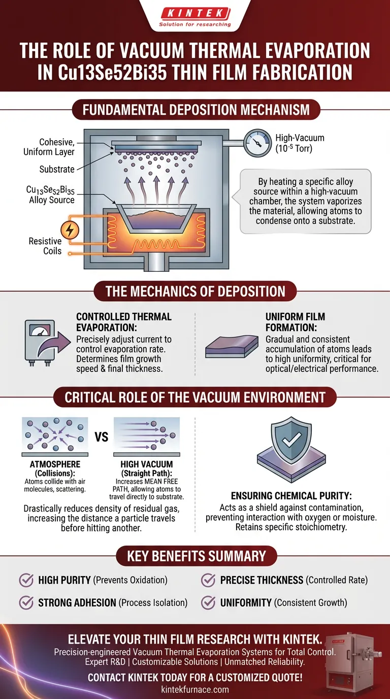
The vacuum thermal evaporation system serves as the fundamental deposition mechanism for fabricating Cu13Se52Bi35 thin films. By heating a specific alloy source within a high-vacuum chamber (typically 10⁻⁵ Torr), the system vaporizes the material, allowing atoms to condense onto a substrate and form a cohesive, uniform layer.
Core Insight The system’s primary value lies in its ability to isolate the deposition process from atmospheric interference. By maximizing the mean free path of particles in a vacuum, it ensures the Cu13Se52Bi35 film achieves high purity, precise thickness, and strong adhesion to the substrate.
The Mechanics of Deposition
To understand how high-quality Cu13Se52Bi35 films are created, one must look at the specific physical controls the system offers.
Controlled Thermal Evaporation
The process begins by applying an electrical current to heat the evaporation source containing the Cu13Se52Bi35 alloy.
Researchers control the evaporation rate by precisely adjusting this current.
This thermal regulation is the primary lever for determining how fast the film grows and its final thickness.
Uniform Film Formation
As the alloy evaporates, atoms travel from the source to the substrate.
Because the rate of evaporation is controlled, the accumulation of atoms is gradual and consistent.
This results in a film with high uniformity, which is critical for the material's subsequent optical or electrical performance.
The Critical Role of the Vacuum Environment
The "vacuum" aspect of the system is not merely for cleanliness; it is a physical requirement for the transport of material.
Increasing the Mean Free Path
In a standard atmosphere, vaporized atoms would instantly collide with air molecules.
The high-vacuum environment (10⁻⁵ Torr) drastically reduces the density of residual gas.
This increases the mean free path—the distance a particle travels before hitting another particle—allowing the Cu13Se52Bi35 atoms to travel in a straight line to the substrate without scattering.
Ensuring Chemical Purity
The vacuum environment acts as a shield against contamination.
It prevents the hot, reactive vapor from interacting with oxygen or moisture present in ambient air.
This ensures that the deposited film retains the specific stoichiometry of the Cu13Se52Bi35 alloy without degradation or oxidation.
Understanding the Trade-offs
While vacuum thermal evaporation is the core method for this material, it is important to recognize the operational constraints.
Directionality and Shadowing
Thermal evaporation is a "line-of-sight" process.
Because atoms travel in straight paths, substrates with complex, three-dimensional geometries may experience "shadowing," where certain areas receive no coating.
Sensitivity to Process Parameters
The quality of the film is strictly tied to the stability of the vacuum and the heating current.
Even minor fluctuations in the vacuum level can shorten the mean free path, leading to reduced deposition efficiency.
Similarly, instability in the heating current can cause variations in the evaporation rate, leading to uneven film thickness or poor adhesion.
Making the Right Choice for Your Goal
When configuring your evaporation system for Cu13Se52Bi35, prioritize parameters based on your specific research objectives.
- If your primary focus is Film Purity: Ensure your system can reliably maintain a base pressure of 10⁻⁵ Torr or lower to eliminate oxidation risks.
- If your primary focus is Thickness Uniformity: Invest in precise current control mechanisms to maintain a stable evaporation rate throughout the deposition cycle.
- If your primary focus is Structural Adhesion: Monitor the substrate preparation and vacuum quality, as these directly influence how well the atoms bond to the surface.
The vacuum thermal evaporation system provides the necessary physical foundation to transform raw alloy into a functional, high-quality thin film.
Summary Table:
| Feature | Role in Cu13Se52Bi35 Fabrication | Key Benefit |
|---|---|---|
| High Vacuum (10⁻⁵ Torr) | Increases mean free path of particles | Prevents oxidation & ensures chemical purity |
| Thermal Regulation | Precisely controls evaporation rate | Consistent film thickness & growth |
| Line-of-Sight Transport | Direct atom-to-substrate condensation | High-purity, cohesive layer formation |
| Process Isolation | Removes atmospheric interference | Enhanced structural adhesion & uniformity |
Elevate Your Thin Film Research with KINTEK
Precision is paramount when fabricating complex alloys like Cu13Se52Bi35. KINTEK provides industry-leading vacuum thermal evaporation systems and lab high-temp furnaces designed to give you total control over deposition parameters.
Why partner with KINTEK?
- Expert R&D: Systems engineered for high-purity results and stable evaporation rates.
- Customizable Solutions: From Muffle and Tube furnaces to advanced CVD and Vacuum systems, we tailor hardware to your unique research needs.
- Unmatched Reliability: Our equipment ensures the high-vacuum stability required for superior thin film adhesion and stoichiometry.
Ready to achieve consistent, high-quality material deposition? Contact KINTEK today for a customized quote!
Visual Guide
References
- Abduelwhab B. Alwany, Abdulnasser Abdulrahman Alfaqeer. Effect of annealing temperature on the structural and optical properties of vacuum evaporated Cu13Se52Bi35 thin films. DOI: 10.15251/cl.2024.211.99
This article is also based on technical information from Kintek Furnace Knowledge Base .
Related Products
- Custom Made Versatile CVD Tube Furnace Chemical Vapor Deposition CVD Equipment Machine
- Vacuum Hot Press Furnace Machine for Lamination and Heating
- Vacuum Heat Treat Sintering and Brazing Furnace
- RF PECVD System Radio Frequency Plasma Enhanced Chemical Vapor Deposition
- Vacuum Heat Treat Furnace with Ceramic Fiber Liner
People Also Ask
- Which industries and research fields benefit from CVD tube furnace sintering systems for 2D materials? Unlock Next-Gen Tech Innovations
- Why are CVD tube furnace sintering systems indispensable for 2D material research and production? Unlock Atomic-Scale Precision
- What customization options are available for CVD tube furnaces? Tailor Your System for Superior Material Synthesis
- How can integrating CVD tube furnaces with other technologies benefit device fabrication? Unlock Advanced Hybrid Processes
- How might AI and machine learning enhance CVD tube furnace processes? Boost Quality, Speed, and Safety


