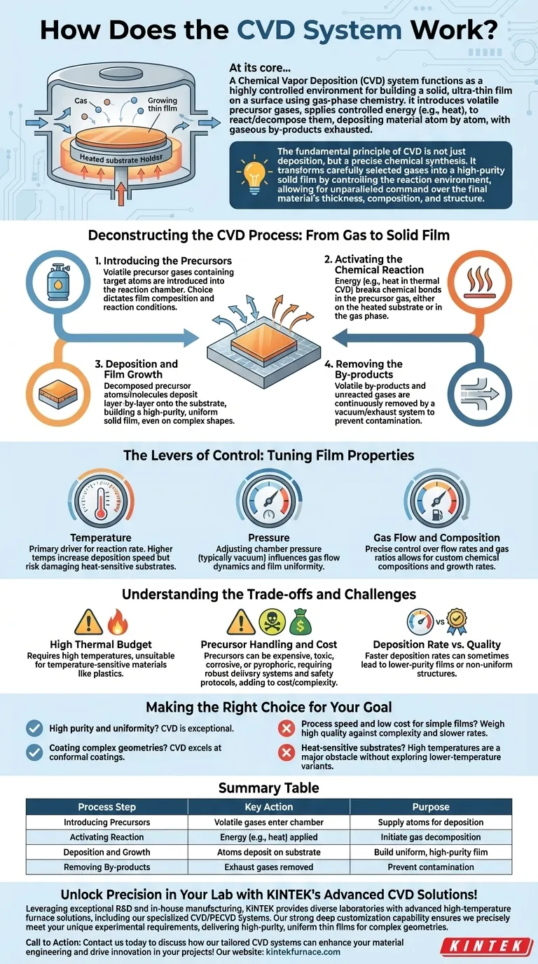
At its core, a Chemical Vapor Deposition (CVD) system functions as a highly controlled environment for building a solid, ultra-thin film on a surface using gas-phase chemistry. It introduces volatile precursor gases into a reaction chamber containing a substrate. Through controlled energy input like heat, these gases react or decompose, depositing a thin layer of material onto the substrate atom by atom, while gaseous by-products are exhausted.
The fundamental principle of CVD is not just deposition, but a precise chemical synthesis. It transforms carefully selected gases into a high-purity solid film by controlling the reaction environment, allowing for unparalleled command over the final material's thickness, composition, and structure.
Deconstructing the CVD Process: From Gas to Solid Film
The entire process can be understood as a sequence of carefully managed physical and chemical events. Each step is critical for achieving a high-quality, uniform coating.
Step 1: Introducing the Precursors
A precursor is a volatile compound containing the atoms you wish to deposit. These are introduced into the reaction chamber as a gas.
The choice of precursor is fundamental, as it dictates the composition of the final film and the reaction conditions required.
Step 2: Activating the Chemical Reaction
Inside the chamber, energy is applied to initiate the chemical reaction. In thermal CVD, the most common type, the substrate is heated to high temperatures.
This heat provides the energy needed to break the chemical bonds in the precursor gas, either on the substrate surface or in the gas phase immediately above it.
Step 3: Deposition and Film Growth
As the precursor gases decompose, the desired solid atoms or molecules deposit onto the surface of the substrate (the material being coated).
This process builds the film layer-by-layer, which allows for uniform coverage even on complex, three-dimensional shapes. The result is a high-purity solid film that is strongly bonded to the substrate.
Step 4: Removing the By-products
The chemical reactions that form the solid film also create volatile by-products. These are unwanted gaseous molecules.
A vacuum or exhaust system continuously removes these by-products and any unreacted precursor gases from the chamber, preventing them from contaminating the growing film.
The Levers of Control: Tuning Film Properties
A CVD system's power lies in its ability to precisely adjust process parameters. These variables act as control levers that directly influence the characteristics of the final film.
Temperature
Temperature is the primary driver for the chemical reaction rate. Higher temperatures generally increase the deposition rate but can also damage heat-sensitive substrates.
Pressure
The process is typically performed under vacuum (below atmospheric pressure). Adjusting the pressure inside the chamber influences gas flow dynamics and the mean free path of molecules, affecting the film's uniformity.
Gas Flow and Composition
Controlling the flow rate and the ratio of different precursor gases allows for precise command over the film's chemical composition and growth rate. This is how custom alloys or doped materials are created.
Understanding the Trade-offs and Challenges
While powerful, CVD is not a universal solution. Understanding its inherent limitations is crucial for successful implementation.
High Thermal Budget
Thermal CVD requires very high temperatures, often hundreds or thousands of degrees Celsius. This makes it unsuitable for coating temperature-sensitive materials like plastics or certain electronic components.
Precursor Handling and Cost
Precursor gases can be expensive, toxic, corrosive, or pyrophoric (igniting on contact with air). They require specialized, robust gas delivery systems and stringent safety protocols, which adds to the operational complexity and cost.
Deposition Rate vs. Quality
There is often a trade-off between the speed of deposition and the quality of the film. Faster deposition rates, achieved through higher temperatures or precursor concentrations, can sometimes lead to lower-purity films or non-uniform structures.
Making the Right Choice for Your Goal
The decision to use CVD depends entirely on the required properties of the final film.
- If your primary focus is high purity and uniformity: CVD is an exceptional choice, as the gas-phase delivery and controlled reactions produce films with very few impurities and excellent thickness control.
- If your primary focus is coating complex geometries: CVD excels at creating conformal coatings that uniformly cover intricate surfaces, a significant advantage over line-of-sight methods like sputtering.
- If your primary focus is process speed and low cost for simple films: You must weigh the high quality of CVD against its operational complexity and potentially slower deposition rates compared to other methods.
- If you are working with heat-sensitive substrates: The high temperatures required for traditional thermal CVD present a major obstacle, making it a poor choice without exploring lower-temperature CVD variants.
By mastering the interplay of gas, heat, and pressure, CVD provides an unparalleled method for engineering materials at the atomic scale.
Summary Table:
| Process Step | Key Action | Purpose |
|---|---|---|
| Introducing Precursors | Volatile gases enter chamber | Supply atoms for deposition |
| Activating Reaction | Energy (e.g., heat) applied | Initiate gas decomposition |
| Deposition and Growth | Atoms deposit on substrate | Build uniform, high-purity film |
| Removing By-products | Exhaust gases removed | Prevent contamination |
Unlock Precision in Your Lab with KINTEK's Advanced CVD Solutions!
Leveraging exceptional R&D and in-house manufacturing, KINTEK provides diverse laboratories with advanced high-temperature furnace solutions, including our specialized CVD/PECVD Systems. Our strong deep customization capability ensures we precisely meet your unique experimental requirements, delivering high-purity, uniform thin films for complex geometries.
Contact us today to discuss how our tailored CVD systems can enhance your material engineering and drive innovation in your projects!
Visual Guide
Related Products
- HFCVD Machine System Equipment for Drawing Die Nano Diamond Coating
- Cylindrical Resonator MPCVD Machine System for Lab Diamond Growth
- Custom Made Versatile CVD Tube Furnace Chemical Vapor Deposition CVD Equipment Machine
- 915MHz MPCVD Diamond Machine Microwave Plasma Chemical Vapor Deposition System Reactor
- MPCVD Machine System Reactor Bell-jar Resonator for Lab and Diamond Growth
People Also Ask
- How can customers maximize the quality of CVD coatings? Master Pre-Coating Prep for Superior Results
- What materials are commonly used in CVD coating systems? Explore Key Materials for Superior Coatings
- What is chemical vapor deposition (CVD) and its primary industrial application? Unlock Precision Thin Films for Electronics
- What are the equipment for chemical vapor deposition? A Guide to the 5 Essential Components
- What role does Chemical Vapor Deposition (CVD) equipment play in the surface coating of carbon fibers for composites?