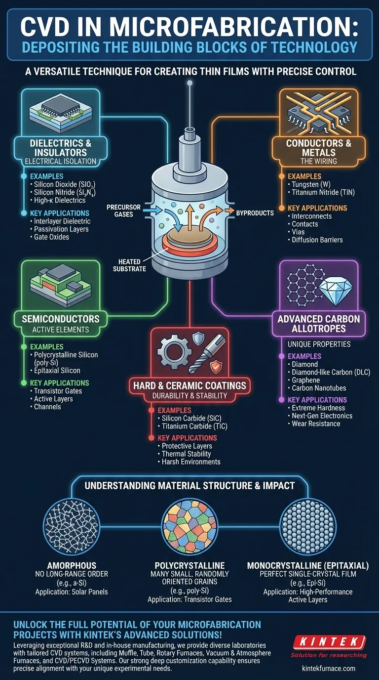
At its core, Chemical Vapor Deposition (CVD) is a remarkably versatile technique capable of depositing a vast range of materials essential for modern microfabrication. These materials fall into three primary categories: electrical insulators (dielectrics) like silicon dioxide, conductive metals like tungsten, and semiconductors like polycrystalline silicon. Beyond these, CVD can also create advanced materials such as diamond, graphene, and various hard ceramic coatings.
The true power of CVD lies not just in the variety of materials it can deposit, but in its precise control over their final structural form—from amorphous to perfect single-crystal films. This control is what allows engineers and scientists to build the complex, layered structures that define modern microelectronic devices.
The Role of CVD in Device Fabrication
Chemical Vapor Deposition is a cornerstone process in manufacturing integrated circuits, MEMS (micro-electromechanical systems), and other micro-scale devices. It is fundamentally a process of building thin films, layer by layer.
How CVD Works in Principle
The process involves introducing precursor gases into a reaction chamber containing the substrate (the wafer). These gases react or decompose on the heated substrate surface, leaving behind a solid thin film of the desired material. The precise control over gas flow, temperature, and pressure allows for highly uniform films with tunable properties.
A Categorical Guide to CVD Materials
The materials deposited by CVD can be best understood by their function within a micro-device.
Dielectrics and Insulators
These materials are used to electrically isolate different conductive layers.
Common examples include silicon dioxide (SiO2), the fundamental insulator in silicon electronics, and silicon nitride (Si3N4), often used as a durable passivation layer and etch mask. For advanced transistors, high-κ dielectrics are deposited to improve performance.
Conductors and Metals
These materials form the "wiring" of a chip, creating interconnects and contacts.
Tungsten (W) is a workhorse metal used to fill small vertical holes (vias) that connect different metal layers. Titanium Nitride (TiN) is a ceramic that is also conductive and is frequently used as a diffusion barrier and adhesion layer beneath other metals.
Semiconductors
These are the active materials that form transistors and other switching elements.
Polycrystalline silicon (poly-Si) is heavily used to create the gate electrodes in transistors. For the highest performance applications, epitaxial silicon is grown, creating a perfect crystal layer on top of the silicon wafer that enables faster electron movement.
Advanced Carbon Allotropes
CVD enables the deposition of pure carbon in various structural forms, each with unique properties.
This includes films of diamond and diamond-like carbon (DLC) for extreme hardness and wear resistance, as well as graphene and carbon nanotubes for next-generation electronics and material science research.
Hard and Ceramic Coatings
For applications requiring high durability, CVD is used to deposit robust ceramic films.
Materials like silicon carbide (SiC) and titanium carbide (TiC) provide exceptional hardness and thermal stability, making them ideal for protective coatings on tools or components used in harsh environments.
Understanding Material Structure and Its Impact
The same material can have vastly different properties depending on its crystalline structure, which CVD can control.
Amorphous Films
Amorphous materials, like amorphous silicon (a-Si), lack a long-range crystalline order. This structure is often used in applications where perfect crystal quality is not needed, such as in large-area electronics like solar panels and flat-panel displays.
Polycrystalline Films
Polycrystalline films are composed of many small, randomly oriented crystal grains. This is the most common form for many materials, including poly-silicon used for transistor gates, offering a good balance between performance and ease of manufacturing.
Monocrystalline and Epitaxial Films
Epitaxial growth produces a single-crystal film that perfectly mimics the crystal structure of the underlying substrate. This defect-free structure allows for the highest possible electron mobility and is reserved for the most performance-critical active layers of a transistor.
Understanding the Trade-offs
While CVD is incredibly powerful, it is not a one-size-fits-all process. The choice of material dictates the entire process and its associated complexity.
Process Conditions are Material-Dependent
Depositing a simple silicon dioxide film can be done at relatively low temperatures. In contrast, growing a high-quality epitaxial silicon or silicon carbide film requires extremely high temperatures and ultra-clean, precisely controlled environments, which significantly increases process complexity and cost.
Film Quality vs. Throughput
There is often a trade-off between the quality of the deposited film and the speed of deposition. Growing a perfect epitaxial layer is a slow, meticulous process, whereas depositing a lower-quality amorphous film can be done much more quickly.
Precursor Chemistry and Safety
Every CVD material requires specific chemical precursors, some of which can be highly toxic, corrosive, or pyrophoric (igniting in air). Managing the handling and disposal of these chemicals is a critical aspect of running a CVD process.
Making the Right Choice for Your Application
Your choice of CVD material and structure is entirely driven by the intended function within the final device.
- If your primary focus is creating active electronic devices: You will rely on high-purity semiconductor films like epitaxial silicon for channels and polycrystalline silicon for gates.
- If your primary focus is electrical isolation or passivation: You will use stable dielectric films such as silicon dioxide (SiO2) or silicon nitride (Si3N4).
- If your primary focus is creating conductive pathways or barriers: You will need metallic films like tungsten (W) for interconnects and titanium nitride (TiN) for diffusion barriers.
- If your primary focus is mechanical protection or thermal stability: You should consider hard ceramic coatings like silicon carbide (SiC) or diamond-like carbon (DLC).
Ultimately, mastering the selection of CVD materials is fundamental to translating a device design into a functional piece of micro-fabricated technology.
Summary Table:
| Material Category | Common Examples | Key Applications |
|---|---|---|
| Dielectrics | Silicon Dioxide (SiO2), Silicon Nitride (Si3N4) | Electrical insulation, passivation layers |
| Conductors | Tungsten (W), Titanium Nitride (TiN) | Interconnects, diffusion barriers |
| Semiconductors | Polycrystalline Silicon, Epitaxial Silicon | Transistor gates, active layers |
| Advanced Carbon | Diamond, Graphene, Carbon Nanotubes | Hard coatings, next-gen electronics |
| Ceramic Coatings | Silicon Carbide (SiC), Titanium Carbide (TiC) | Protective layers, thermal stability |
Unlock the full potential of your microfabrication projects with KINTEK's advanced high-temperature furnace solutions! Leveraging exceptional R&D and in-house manufacturing, we provide diverse laboratories with tailored CVD systems, including Muffle, Tube, Rotary Furnaces, Vacuum & Atmosphere Furnaces, and CVD/PECVD Systems. Our strong deep customization capability ensures precise alignment with your unique experimental needs, enabling superior material deposition for enhanced device performance and efficiency. Contact us today to discuss how our solutions can drive your innovations forward!
Visual Guide
Related Products
- HFCVD Machine System Equipment for Drawing Die Nano Diamond Coating
- Cylindrical Resonator MPCVD Machine System for Lab Diamond Growth
- Custom Made Versatile CVD Tube Furnace Chemical Vapor Deposition CVD Equipment Machine
- 915MHz MPCVD Diamond Machine Microwave Plasma Chemical Vapor Deposition System Reactor
- RF PECVD System Radio Frequency Plasma Enhanced Chemical Vapor Deposition
People Also Ask
- What is the advantage of using a CVD system for coating turbine blades? Master Complex Geometries with Ease
- What core function does CVD equipment serve in h-BN anti-corrosion? Master Precision Synthesis for High-Performance Films
- What are the equipment for chemical vapor deposition? A Guide to the 5 Essential Components
- What is the function of high-purity Argon (Ar) gas during CVD? Optimize Your Thin Film Uniformity and Purity
- What is the significance of the vacuum pressure control system in the CVD coating process for powders?