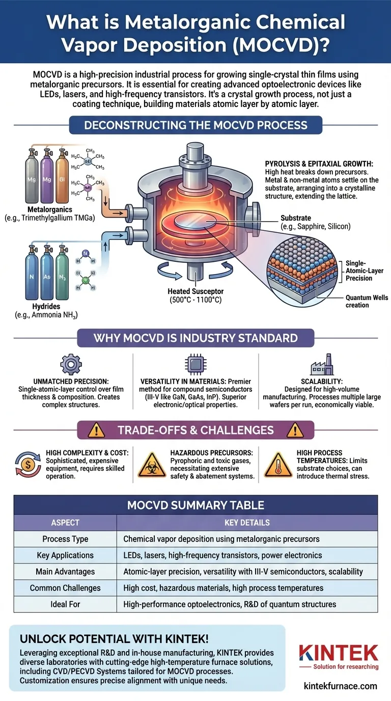
In short, Metalorganic Chemical Vapor Deposition (MOCVD) is a highly precise industrial process for growing high-quality, single-crystal thin films. It is a specific type of chemical vapor deposition (CVD) that uses metalorganic compounds as precursor gases to deposit complex semiconductor materials, which are the building blocks of devices like LEDs, lasers, and high-frequency transistors.
MOCVD is not simply a coating technique; it is a crystal growth process. Its fundamental value lies in its ability to build complex semiconductor materials one atomic layer at a time, enabling the creation of advanced electronic and optoelectronic devices that would otherwise be impossible to manufacture.
Deconstructing the MOCVD Process
To understand MOCVD, it's best to break it down into its core components. The process is a carefully orchestrated chemical reaction occurring within a highly controlled environment.
The Role of the Reactor
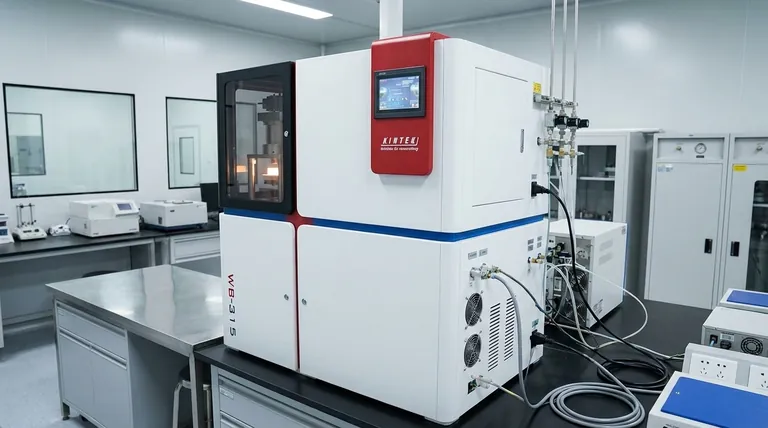
The entire process takes place inside a reaction chamber, typically under vacuum or controlled pressure. A substrate wafer, often made of sapphire, silicon, or another semiconductor, is placed on a rotating platter called a susceptor. This susceptor is heated to very high temperatures, often between 500°C and 1100°C.
Introducing the Precursors
The "magic" of MOCVD comes from its chemical ingredients, known as precursors. These are highly pure gases that carry the atoms needed for the final film.
- Metalorganics: These are compounds where a metal atom (like Gallium, Indium, or Aluminum) is chemically bonded to organic molecules. For example, Trimethylgallium (TMGa) is a gas that carries Gallium atoms. These are used because they are volatile (easily turned into a gas) and can be controlled with extreme precision.
- Hydrides: Other gases, like ammonia (NH₃) or arsine (AsH₃), are used to provide the non-metal elements (Nitrogen or Arsenic).
These gases are precisely mixed and injected into the reactor.
The Chemical Reaction on the Substrate
When the precursor gases flow over the hot substrate, the intense heat causes them to break apart in a process called pyrolysis. The organic molecules are stripped away, releasing the metal atoms.
These newly freed metal and non-metal atoms then settle onto the hot substrate surface. The surface provides a template, and the atoms arrange themselves into a highly ordered, crystalline structure, extending the crystal lattice of the substrate. This is known as epitaxial growth.
Why MOCVD is the Industry Standard for Optoelectronics
MOCVD is not the only way to create thin films, but it dominates specific, high-value applications for several key reasons. It is fundamentally different from physical deposition methods, which essentially sputter or evaporate material onto a surface.
Unmatched Precision and Control
By precisely controlling the gas flow rates, temperature, and pressure, engineers can control the film's thickness and composition with single-atomic-layer precision. This allows for the creation of complex, layered structures like quantum wells, which are essential for tuning the color and efficiency of an LED.
Versatility in Compound Semiconductors
MOCVD is the premier method for growing compound semiconductors, especially III-V materials like Gallium Nitride (GaN), Gallium Arsenide (GaAs), and Indium Phosphide (InP). These materials have superior electronic and optical properties compared to silicon and are the basis for all modern solid-state lighting and laser diodes.
Scalability for Mass Production
While complex, MOCVD reactors are designed for high-volume manufacturing. Modern systems can process multiple large-diameter wafers (e.g., 6-inch or 8-inch) in a single run, making it an economically viable process for mass-producing LEDs and other devices.
Understanding the Trade-offs and Challenges
Despite its power, MOCVD is not a universal solution. Its application is specialized due to significant practical challenges.
High Complexity and Cost
MOCVD reactors are incredibly sophisticated and expensive pieces of capital equipment, costing millions of dollars. They require extensive support facilities and highly trained personnel to operate and maintain.
Hazardous Precursor Materials
The metalorganic and hydride gases used in MOCVD are extremely dangerous. Many are pyrophoric (ignite spontaneously on contact with air) and highly toxic. This necessitates extensive safety monitoring systems, gas cabinets, and abatement systems to neutralize exhaust gases, adding to the cost and complexity.
High Process Temperatures
The high temperatures required can limit the types of substrates that can be used. It can also introduce thermal stress into the material, which must be carefully managed to prevent cracking and defects in the final film.
Making the Right Choice for Your Goal
Selecting a deposition technology depends entirely on the material requirements of your final application.
- If your primary focus is high-performance LEDs, lasers, or power electronics: MOCVD is the established, non-negotiable industry standard due to its atomic-level control over compound semiconductor alloys.
- If your primary focus is research and development of novel quantum structures: MOCVD provides the flexibility and precision needed to create and test new material compositions and device architectures.
- If your primary focus is a simple protective or conductive coating on metal or glass: MOCVD is overkill. Simpler, cheaper, and safer methods like sputtering (a PVD technique) or general-purpose CVD are far more appropriate.
Ultimately, MOCVD is the enabling technology behind the solid-state lighting revolution and much of the high-frequency communications we rely on today.
Summary Table:
| Aspect | Key Details |
|---|---|
| Process Type | Chemical vapor deposition using metalorganic precursors |
| Key Applications | LEDs, lasers, high-frequency transistors, power electronics |
| Main Advantages | Atomic-layer precision, versatility with III-V semiconductors, scalability for mass production |
| Common Challenges | High cost, hazardous materials, high process temperatures |
| Ideal For | High-performance optoelectronics, R&D of quantum structures |
Unlock the potential of advanced semiconductor manufacturing with KINTEK! Leveraging exceptional R&D and in-house manufacturing, we provide diverse laboratories with cutting-edge high-temperature furnace solutions, including CVD/PECVD Systems tailored for MOCVD processes. Our strong deep customization capability ensures precise alignment with your unique experimental needs, whether you're developing next-generation LEDs, lasers, or other optoelectronic devices. Contact us today to discuss how our expertise can enhance your research and production efficiency!
Visual Guide
Related Products
- Cylindrical Resonator MPCVD Machine System for Lab Diamond Growth
- 915MHz MPCVD Diamond Machine Microwave Plasma Chemical Vapor Deposition System Reactor
- MPCVD Machine System Reactor Bell-jar Resonator for Lab and Diamond Growth
- Multi Heating Zones CVD Tube Furnace Machine for Chemical Vapor Deposition Equipment
- HFCVD Machine System Equipment for Drawing Die Nano Diamond Coating
People Also Ask
- What factors influence the quality of diamond deposition in the MPCVD method? Master the Critical Parameters for High-Quality Diamond Growth
- What are the key components of an MPCVD system? Unlock High-Purity Crystal Growth
- How does MPCVD achieve stable temperature control during diamond growth? Master Precise Thermal Management
- How does pressure affect the MPCVD growth process? Master Plasma Control for Superior Film Quality
- What are the essential components of an MPCVD reactor system? Build a Pristine Environment for High-Purity Materials


