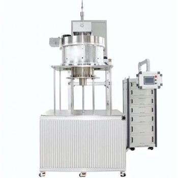
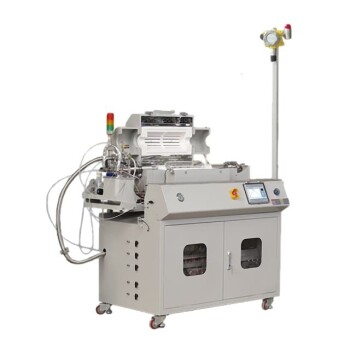
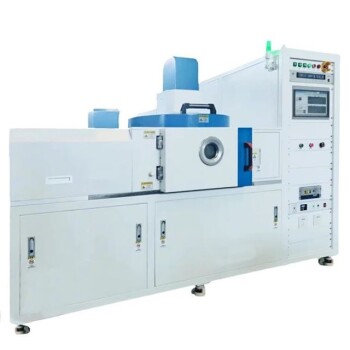
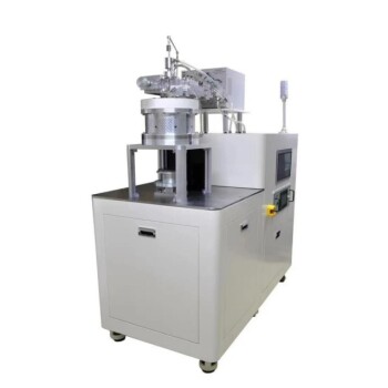
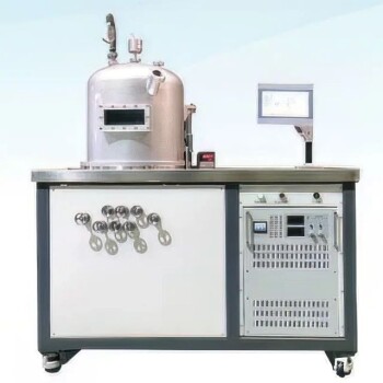
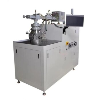
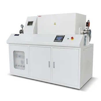
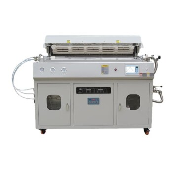
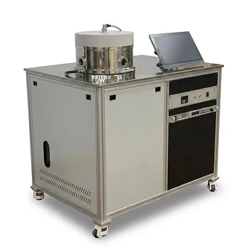
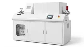
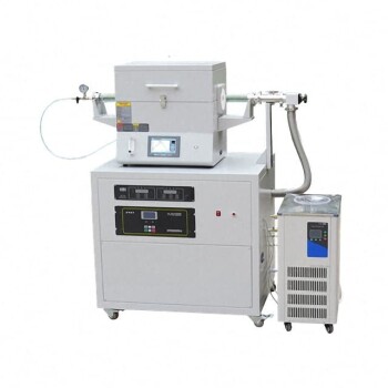
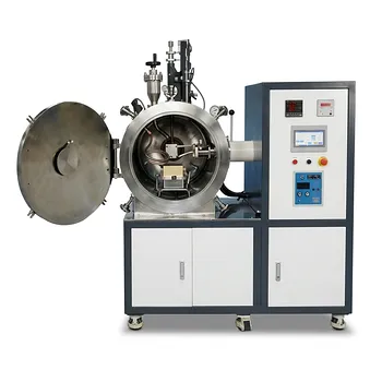
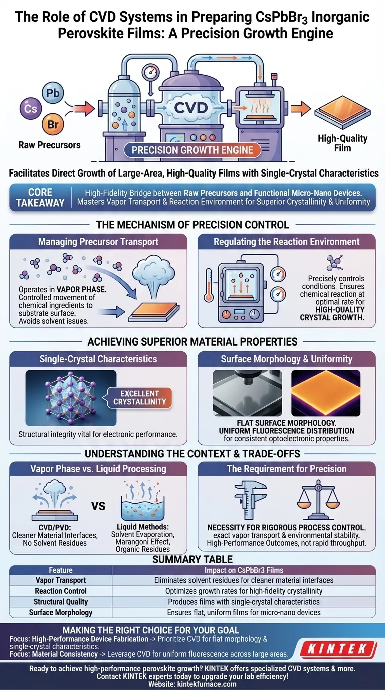
A Chemical Vapor Deposition (CVD) system serves as a precision growth engine for preparing CsPbBr3 inorganic perovskite films. It facilitates the direct growth of large-area, high-quality films that exhibit single-crystal characteristics on a target substrate.
Core Takeaway The CVD system functions as a high-fidelity bridge between raw precursors and functional micro-nano devices. By mastering the vapor transport and reaction environment, it produces CsPbBr3 films with superior crystallinity and surface uniformity that are difficult to achieve through standard solution-based methods.
The Mechanism of Precision Control
Managing Precursor Transport
The fundamental role of the CVD system is to manage the transport of precursor vapors.
Unlike liquid methods where precursors are dissolved in solvents, CVD operates in the vapor phase. This allows for the controlled movement of chemical ingredients to the substrate surface.
Regulating the Reaction Environment
Success in growing inorganic perovskites relies on a stable reaction environment.
The CVD system allows you to precisely control the conditions under which the CsPbBr3 forms. This regulation ensures the chemical reaction occurs at the optimal rate for high-quality crystal growth.
Achieving Superior Material Properties
Single-Crystal Characteristics
The most significant output of a properly tuned CVD process is the structural quality of the film.
The system enables the growth of films with excellent crystallinity, often possessing characteristics similar to single crystals. This structural integrity is vital for the electronic performance of the final material.
Surface Morphology and Uniformity
For micro-nano devices, the physical landscape of the film is as important as its internal structure.
CVD systems produce films with a flat surface morphology. Furthermore, they ensure a uniform fluorescence distribution, indicating that the optoelectronic properties are consistent across the entire large-area film.
Understanding the Context and Trade-offs
Vapor Phase vs. Liquid Processing
While liquid-based methods (like inkjet printing) focus on managing solvent evaporation and preventing effects like the Marangoni effect, vapor deposition takes a different approach.
CVD, similar to Physical Vapor Deposition (PVD), operates in a regime that avoids organic solvent residues. This eliminates "solvent-induced etching" problems often found in liquid processing, resulting in cleaner material interfaces.
The Requirement for Precision
The primary trade-off of using a CVD system is the necessity for rigorous process control.
Because the system relies on the exact transport of vapors and environmental stability, deviation in these parameters can disrupt the growth of single-crystal characteristics. It is a method designed for high-performance outcomes rather than rapid, low-fidelity throughput.
Making the Right Choice for Your Goal
If your primary focus is High-Performance Device Fabrication: Prioritize CVD to obtain the flat morphology and single-crystal characteristics required for efficient micro-nano devices.
If your primary focus is Material Consistency: Leverage the CVD system's ability to create uniform fluorescence distribution across large areas, ensuring reliable performance data.
The CVD system transforms volatile precursors into a robust, high-quality material platform essential for advanced inorganic perovskite applications.
Summary Table:
| Feature | Impact on CsPbBr3 Films |
|---|---|
| Vapor Transport | Eliminates solvent residues for cleaner material interfaces |
| Reaction Control | Optimizes growth rates for high-fidelity crystallinity |
| Structural Quality | Produces films with single-crystal characteristics |
| Surface Morphology | Ensures flat, uniform films for micro-nano devices |
Ready to achieve high-performance perovskite growth?
Backed by expert R&D and manufacturing, KINTEK offers specialized CVD systems, Tube, Rotary, Vacuum, and Muffle furnaces, all customizable for your unique lab requirements. Our technology empowers you to master vapor transport and reaction environments to produce superior CsPbBr3 films with unmatched consistency.
Contact KINTEK experts today to upgrade your lab efficiency!
Visual Guide
References
- Qi Han, Ji Li. Inorganic perovskite-based active multifunctional integrated photonic devices. DOI: 10.1038/s41467-024-45565-9
This article is also based on technical information from Kintek Furnace Knowledge Base .
Related Products
- 915MHz MPCVD Diamond Machine Microwave Plasma Chemical Vapor Deposition System Reactor
- Custom Made Versatile CVD Tube Furnace Chemical Vapor Deposition CVD Equipment Machine
- RF PECVD System Radio Frequency Plasma Enhanced Chemical Vapor Deposition
- MPCVD Machine System Reactor Bell-jar Resonator for Lab and Diamond Growth
- HFCVD Machine System Equipment for Drawing Die Nano Diamond Coating
People Also Ask
- What is the MPCVD method and why is it considered effective for diamond deposition? Superior Purity & High Growth Rates
- What factors influence the quality of diamond deposition in the MPCVD method? Master the Critical Parameters for High-Quality Diamond Growth
- What are some key features and benefits of the microwave plasma chemical vapor deposition system? Achieve Unmatched Material Synthesis
- What is the purpose of a microwave plasma chemical vapor deposition system? Grow High-Purity Diamonds and Advanced Materials
- What is the basic principle of operation for the microwave plasma chemical vapor deposition system? Unlock High-Purity Material Growth