In short, Chemical Vapor Deposition (CVD) is a cornerstone technology used across high-tech industries to create exceptionally thin, high-performance coatings. Its primary applications are in manufacturing semiconductors and integrated circuits, applying protective wear-resistant coatings for aerospace and automotive parts, and creating biocompatible surfaces for medical implants.
The true value of CVD is not in any single application, but in its fundamental ability to build materials atom by atom. This allows for the creation of ultra-pure, perfectly uniform films that give ordinary surfaces extraordinary properties.
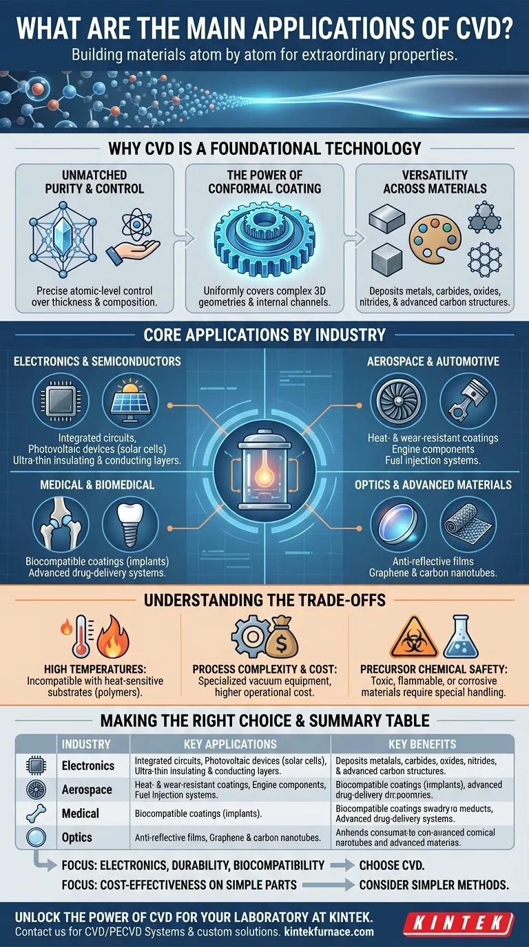
Why CVD is a Foundational Technology
Before looking at specific products, it’s critical to understand what makes the CVD process so uniquely powerful. Its advantages are the reason it has been adopted in so many demanding fields.
Unmatched Purity and Control
CVD allows for the deposition of films with extremely high purity. The process gives engineers precise, atomic-level control over the thickness and chemical composition of the coating, ensuring consistent performance.
The Power of Conformal Coating
A key advantage of CVD is its ability to create conformal coatings. This means the film perfectly and uniformly covers every surface of an object, including complex, three-dimensional geometries and internal channels that are impossible to coat with traditional line-of-sight methods.
Versatility Across Materials
The CVD process is not limited to a single type of material. It is highly versatile and can be used to deposit a wide range of substances, including metals, hard carbides, stable oxides, nitrides, and advanced carbon structures like graphene.
Core Applications by Industry
This unique combination of control, conformity, and versatility allows CVD to solve critical challenges across several key industries.
Electronics and Semiconductors
This is arguably the most significant application of CVD. The entire digital world is built on silicon chips, which rely on CVD to deposit the ultra-thin insulating, conducting, and semiconducting layers that form integrated circuits. It's also used to create the efficient layers in photovoltaic devices (solar cells).
Aerospace and Automotive
In environments defined by high heat and extreme friction, CVD provides critical protection. It's used to apply heat- and wear-resistant coatings on jet engine turbine blades and durable, low-friction coatings on automotive engine components and fuel injection systems, improving longevity and fuel efficiency.
Medical and Biomedical
When a material must safely interact with the human body, CVD is essential. It's used to apply inert, biocompatible coatings on medical implants like artificial joints and dental implants to prevent rejection. The technology is also being explored for advanced drug-delivery systems.
Optics and Advanced Materials
CVD is used to apply specialized coatings on lenses and optical instruments, such as anti-reflective films. Beyond this, it is a primary method for producing cutting-edge materials like graphene and carbon nanotubes, which have unique thermal, mechanical, and electrical properties for next-generation applications.
Understanding the Trade-offs
While powerful, CVD is not a universal solution. Its precision comes with specific constraints that make it unsuitable for certain applications.
High Temperatures and Substrate Limits
Many CVD processes require very high temperatures, often several hundred degrees Celsius. This makes the process incompatible with heat-sensitive substrate materials, such as many polymers or plastics.
Process Complexity and Cost
CVD is a sophisticated, vacuum-based process that requires specialized equipment and careful control of precursor gases. This complexity makes it significantly more expensive than simpler coating methods like painting or electroplating, especially for large-scale production.
Precursor Chemical Safety
The "vapor" in Chemical Vapor Deposition comes from precursor chemicals, which can be toxic, flammable, or corrosive. These materials require specialized handling, storage, and safety protocols, adding to the operational overhead.
Making the Right Choice for Your Goal
Selecting CVD depends entirely on whether its unique capabilities justify its complexity and cost for your specific objective.
- If your primary focus is electronic performance and precision: CVD is the non-negotiable industry standard for creating the pure, uniform films required for semiconductors.
- If your primary focus is durability in harsh environments: CVD provides unmatched heat, corrosion, and wear resistance for critical aerospace and automotive components.
- If your primary focus is biocompatibility: CVD is the proven method for creating safe, inert surfaces on medical devices that will be placed inside the human body.
- If your primary focus is cost-effectiveness on simple parts: For non-critical applications that don't require atomic precision or conformal coating, simpler methods are often more practical.
Ultimately, CVD empowers engineers and scientists to design materials from the atom up, redefining performance across countless industries.
Summary Table:
| Industry | Key Applications | Key Benefits |
|---|---|---|
| Electronics & Semiconductors | Integrated circuits, solar cells | High purity, precise control, uniform films |
| Aerospace & Automotive | Turbine blades, engine components | Wear resistance, heat protection, longevity |
| Medical & Biomedical | Implants, drug-delivery systems | Biocompatibility, safety, inert surfaces |
| Optics & Advanced Materials | Anti-reflective films, graphene | Conformal coating, versatility, unique properties |
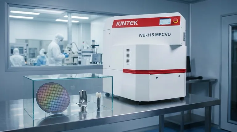
Unlock the Power of CVD for Your Laboratory
At KINTEK, we specialize in providing advanced high-temperature furnace solutions, including our CVD/PECVD Systems, to help you achieve precise, high-performance coatings. Leveraging exceptional R&D and in-house manufacturing, we offer deep customization to meet your unique experimental needs in semiconductors, aerospace, medical devices, and more.
Contact us today to discuss how our tailored solutions can enhance your research and production efficiency!
Visual Guide
Related Products
- Custom Made Versatile CVD Tube Furnace Chemical Vapor Deposition CVD Equipment Machine
- Multi Heating Zones CVD Tube Furnace Machine for Chemical Vapor Deposition Equipment
- HFCVD Machine System Equipment for Drawing Die Nano Diamond Coating
- Split Chamber CVD Tube Furnace with Vacuum Station CVD Machine
- 915MHz MPCVD Diamond Machine Microwave Plasma Chemical Vapor Deposition System Reactor
People Also Ask
- What are the practical applications of gate media prepared by CVD tube furnaces? Unlock Advanced Electronics and More
- Why are CVD tube furnace sintering systems indispensable for 2D material research and production? Unlock Atomic-Scale Precision
- How does CVD tube furnace sintering enhance graphene growth? Achieve Superior Crystallinity and High Electron Mobility
- What future trends are expected in the development of CVD tube furnaces? Discover Smarter, More Versatile Systems
- What temperature range do standard CVD tube furnaces operate at? Unlock Precision for Your Material Deposition


