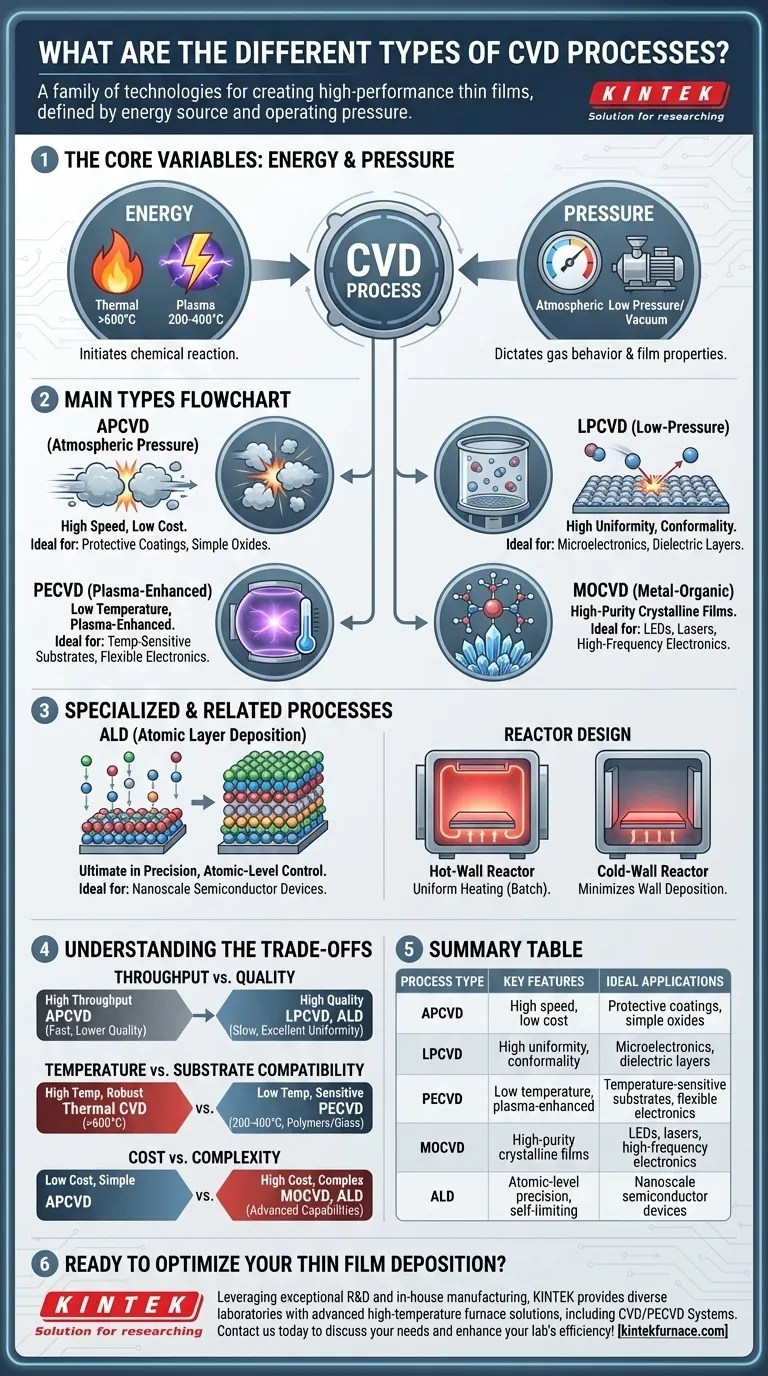
At its core, Chemical Vapor Deposition (CVD) is not a single process but a family of technologies for creating high-performance thin films. The primary types are distinguished by their energy source and operating pressure, including Atmospheric Pressure CVD (APCVD) for high-speed deposition, Low-Pressure CVD (LPCVD) for high uniformity, Plasma-Enhanced CVD (PECVD) for low-temperature processing, and Metal-Organic CVD (MOCVD) for creating specific crystalline materials.
The "best" CVD process does not exist. The critical decision is a strategic trade-off between film quality, deposition speed, processing temperature, and cost, with each variant optimized to solve a different engineering problem.
The Core Variables: Energy and Pressure
Understanding any CVD process begins with two fundamental parameters: the energy used to initiate the chemical reaction and the pressure inside the reaction chamber. These two factors dictate nearly everything about the final film's properties.
H3: Thermal CVD: The Foundation
Thermal CVD is the most fundamental form of the process. It uses high temperatures (often >600°C) to provide the activation energy needed for precursor gases to react and deposit onto a substrate.
This method is conceptually simple and can produce very pure, high-quality films. Its main limitation is the high temperature, which can damage or warp sensitive substrates, such as those with existing integrated circuits.
H3: Plasma-Enhanced CVD (PECVD): The Low-Temperature Solution
PECVD overcomes the temperature limitations of thermal CVD. Instead of relying solely on heat, it uses an electric field to generate a plasma, an ionized gas.
This plasma provides the energy to break down the precursor gases at much lower temperatures (typically 200-400°C). This makes PECVD essential for depositing films on temperature-sensitive materials like plastics or fully fabricated semiconductor wafers.
How Operating Pressure Defines the Process
The pressure inside the reactor chamber dramatically affects how gas molecules travel and react, directly influencing the quality and uniformity of the deposited film.
H3: Atmospheric Pressure CVD (APCVD): For Speed and Throughput
APCVD operates at standard atmospheric pressure. This eliminates the need for expensive and slow vacuum pumping systems, making the process fast and cost-effective.
However, at this pressure, gas molecules collide frequently. This can lead to unwanted reactions in the gas phase before they reach the substrate, potentially reducing film quality and uniformity. It is best suited for applications where high throughput is more critical than perfect film structure.
H3: Low-Pressure CVD (LPCVD): For Quality and Conformality
LPCVD operates under a vacuum (well below atmospheric pressure). This increases the mean free path of the gas molecules, meaning they travel further before colliding.
As a result, reactions are dominated by what happens on the substrate surface, not in the gas above it. This leads to films with excellent uniformity and conformality—the ability to evenly coat complex, three-dimensional structures. It is a workhorse of the semiconductor industry.
Specialized Processes for Advanced Needs
As technology demands more from materials, specialized CVD variants have been developed to meet highly specific requirements.
H3: Metal-Organic CVD (MOCVD): For High-Purity Crystalline Films
MOCVD is a specific type of thermal CVD that uses metal-organic precursors—complex molecules containing a metal atom bonded to organic groups.
This process is the industry standard for manufacturing high-quality compound semiconductors, such as the gallium arsenide (GaAs) and gallium nitride (GaN) used in LEDs, lasers, and high-frequency electronics. The choice of precursor gives precise control over the final material's composition.
H3: Atomic Layer Deposition (ALD): The Ultimate in Precision
Often considered a subclass of CVD, ALD takes precision to the atomic level. Instead of a continuous flow of gases, ALD uses sequential, self-limiting pulses of different precursors.
Each pulse deposits exactly one atomic layer and will not deposit more, regardless of exposure time. This provides unparalleled, angstrom-level control over film thickness, which is absolutely critical for modern, nanoscale semiconductor devices.
H3: Reactor Design: Hot-Wall vs. Cold-Wall
The reactor configuration also defines the process. In a hot-wall reactor, the chamber walls are heated along with the substrate, which is ideal for uniform heating in batch processing. In a cold-wall reactor, only the substrate is heated, minimizing unwanted film deposition on the chamber walls.
Understanding the Trade-offs
Choosing a CVD process involves balancing competing priorities. No single method is superior in all aspects; each represents a different optimization point.
H3: Throughput vs. Quality
APCVD offers the highest throughput but often at the cost of film purity and uniformity. In contrast, LPCVD and ALD deliver exceptional quality and conformality but are significantly slower processes.
H3: Temperature vs. Substrate Compatibility
Thermal CVD is simple but its high temperatures limit it to robust substrates like silicon wafers. PECVD's key advantage is its low deposition temperature, enabling its use on polymers, glass, and devices that cannot withstand thermal stress.
H3: Cost vs. Complexity
APCVD systems are generally the simplest and least expensive. LPCVD and PECVD systems require vacuum equipment, increasing cost. MOCVD and ALD systems are highly complex and expensive, reserved for applications where their unique capabilities in material quality or thickness control are non-negotiable.
Selecting the Right CVD Process for Your Goal
Your application's primary requirement will guide your choice of technology.
- If your primary focus is maximum throughput and low cost: APCVD is your starting point for applications like depositing protective coatings or simple oxide layers.
- If your primary focus is high uniformity and coating complex shapes: LPCVD is the industry standard for critical dielectric and polysilicon layers in microelectronics.
- If your primary focus is depositing on temperature-sensitive substrates: PECVD is the necessary choice for applications involving plastics, completed circuits, or flexible electronics.
- If your primary focus is growing high-purity crystalline films for optoelectronics: MOCVD is the specialized tool required for manufacturing LEDs, lasers, and high-power transistors.
- If your primary focus is ultimate thickness control at the atomic scale: ALD is the only process that provides the angstrom-level precision needed for cutting-edge logic and memory chips.
Ultimately, choosing the right deposition technology is about clearly defining your material needs and selecting the tool that meets them most effectively.
Summary Table:
| Process Type | Key Features | Ideal Applications |
|---|---|---|
| APCVD | High speed, low cost | Protective coatings, simple oxides |
| LPCVD | High uniformity, conformality | Microelectronics, dielectric layers |
| PECVD | Low temperature, plasma-enhanced | Temperature-sensitive substrates, flexible electronics |
| MOCVD | High-purity crystalline films | LEDs, lasers, high-frequency electronics |
| ALD | Atomic-level precision, self-limiting | Nanoscale semiconductor devices |
Ready to optimize your thin film deposition? Leveraging exceptional R&D and in-house manufacturing, KINTEK provides diverse laboratories with advanced high-temperature furnace solutions. Our product line, including Muffle, Tube, Rotary Furnaces, Vacuum & Atmosphere Furnaces, and CVD/PECVD Systems, is complemented by our strong deep customization capability to precisely meet unique experimental requirements. Whether you're working with semiconductors, optoelectronics, or other materials, we can help you select and customize the ideal CVD process for superior results. Contact us today to discuss your needs and enhance your lab's efficiency!
Visual Guide
Related Products
- MPCVD Machine System Reactor Bell-jar Resonator for Lab and Diamond Growth
- Custom Made Versatile CVD Tube Furnace Chemical Vapor Deposition CVD Equipment Machine
- 915MHz MPCVD Diamond Machine Microwave Plasma Chemical Vapor Deposition System Reactor
- Cylindrical Resonator MPCVD Machine System for Lab Diamond Growth
- Slide PECVD Tube Furnace with Liquid Gasifier PECVD Machine
People Also Ask
- How does pressure affect the MPCVD growth process? Master Plasma Control for Superior Film Quality
- What are the key components of an MPCVD system? Unlock High-Purity Crystal Growth
- What role does gas flow rate play in MPCVD? Mastering Deposition Rate and Film Uniformity
- Why is temperature control important in the MPCVD growth process? Ensure High-Quality, Reliable Diamond Film Deposition
- What are the essential components of an MPCVD reactor for diamond film deposition? Unlock High-Quality Diamond Growth