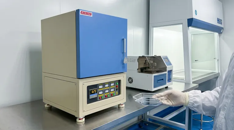
The primary technical objective of performing thermal oxidation at 625 °C is to achieve precision thickness control. This specific thermal environment enables the growth of an ultra-thin silicon oxide (SiOx) layer, typically measuring approximately 1.5 nm. By maintaining this exact temperature in an oxygen environment, the process ensures the layer is uniform enough to passivate the surface while remaining thin enough to permit efficient charge carrier transport via the tunneling effect.
The 625 °C oxidation process is designed to achieve a critical structural balance: creating a layer uniform enough to chemically protect the silicon surface, yet thin enough to remain electrically conductive through quantum tunneling.
The Mechanics of Controlled Oxidation
Achieving Ultra-Thin Dimensions
The central goal of this thermal process is to limit oxide growth to the nanometer scale.
At 625 °C, the oxidation rate is sufficiently controlled to stop growth at approximately 1.5 nm. This specific thickness is the threshold required to create a functional tunnel oxide layer rather than a standard insulating gate oxide.
Ensuring Superior Uniformity
Creating a layer this thin is difficult without introducing structural inconsistencies.
The 625 °C oxygen environment facilitates superior uniformity across the silicon surface. A uniform layer is essential for consistent device performance, preventing weak spots where the oxide might fail or break down prematurely.
Enabling Surface Passivation
A key function of the SiOx layer is to reduce surface defects that can trap charge carriers.
The uniformity achieved at this temperature ensures effective surface passivation. This reduces the recombination of electrons and holes at the interface, which is vital for maintaining the electrical efficiency of the underlying silicon.
Facilitating the Tunneling Effect
The defining characteristic of a "tunnel" oxide is its ability to allow current to pass through it.
Because the layer is restricted to ~1.5 nm, it allows for the efficient transport of charge carriers. This occurs through quantum tunneling, where carriers pass through the barrier rather than climbing over it, a mechanism impossible with thicker oxide layers.
Understanding the Process Trade-offs
The Thickness vs. Protection Balance
The technical challenge lies in the opposing requirements of passivation and conductivity.
If the temperature varies significantly, the oxide may grow too thick, blocking the tunneling effect and insulating the device. Conversely, an inconsistent thermal environment may yield a layer with poor uniformity, compromising its ability to provide adequate surface passivation. The 625 °C setpoint is the specific calibration used to satisfy both requirements simultaneously without favoring one to the detriment of the other.
Optimizing for Device Performance
To apply this to your fabrication process, you must evaluate your specific device requirements against the properties of the oxide layer.
- If your primary focus is Carrier Transport: Ensure strict adherence to the 625 °C limit to prevent the layer from exceeding the 1.5 nm tunneling threshold.
- If your primary focus is Surface Quality: Prioritize the stability of the oxygen environment to guarantee the uniformity required for effective passivation.
Precision at this stage is the difference between a highly efficient tunnel junction and a resistive barrier.
Summary Table:
| Feature | Technical Specification | Functional Objective |
|---|---|---|
| Target Temperature | 625 °C | Controlled, ultra-slow oxidation rate |
| Oxide Thickness | ~1.5 nm | Threshold for quantum tunneling effect |
| Environment | Oxygen (O2) | Superior chemical uniformity and passivation |
| Main Benefit | Charge Transport | High carrier efficiency with low recombination |
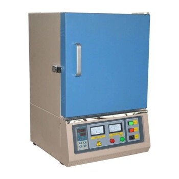
Elevate Your Semiconductor Fabrication with KINTEK
Precision at the nanometer scale requires absolute thermal control. Backed by expert R&D and manufacturing, KINTEK offers a wide range of lab high-temp furnaces, including Muffle, Tube, and Vacuum systems specifically designed for high-accuracy thermal oxidation and CVD processes. Whether you are developing SiOx tunnel layers or advanced electronic components, our customizable systems provide the uniformity and stability your research demands.
Ready to optimize your thin-film growth? Contact KINTEK today to discuss your custom furnace requirements with our technical experts.
References
- TiN <sub> <i>x</i> </sub> and TiO <sub> <i>x</i> </sub> /TiN <sub> <i>x</i> </sub> Barrier Layers for Al‐Based Metallization of Passivating Contacts in Si Solar Cells. DOI: 10.1002/pssr.202500168
This article is also based on technical information from Kintek Furnace Knowledge Base .
Related Products
- 1700℃ Controlled Inert Nitrogen Atmosphere Furnace
- 1400℃ Muffle Oven Furnace for Laboratory
- Mesh Belt Controlled Atmosphere Furnace Inert Nitrogen Atmosphere Furnace
- 1200℃ Controlled Inert Nitrogen Atmosphere Furnace
- Controlled Inert Nitrogen Hydrogen Atmosphere Furnace
People Also Ask
- What role does a high-temperature inert atmosphere furnace play in carbonization? Optimize Your Carbon Yield
- How are inert atmosphere furnaces sealed and prepared for operation? Ensure Process Integrity and Prevent Oxidation
- How are inert atmosphere furnaces used in the ceramics industry? Ensure Purity and Performance in High-Temp Processing
- How is atmosphere control managed during furnace operation? Master Precise Gas Environments for Superior Results
- How does a chemically inert atmosphere function in a furnace? Prevent Oxidation and Ensure Material Purity