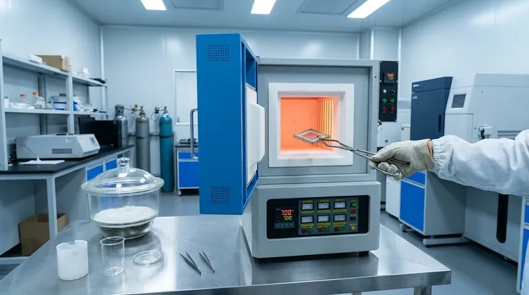
The primary role of the laboratory high-temperature annealing furnace in this context is to induce a specific structural phase transition that creates stable, amorphous (InxGa1-x)2O3 (IGO) thin films. By subjecting spin-coated samples to a precise thermal treatment of 700 °C for 30 minutes, the furnace drives the removal of organic impurities and converts the precursor sol into a solidified gel state.
Core Insight: Unlike many semiconductor processes where annealing is used to achieve perfect crystallinity, this specific process uses heat to induce lattice distortion. This transforms the crystalline Ga2O3 phase into a highly functional amorphous structure, significantly increasing oxygen vacancy concentrations to enhance material performance.
Mechanisms of Film Transformation
The Sol-Gel Transition and Purification
The initial function of the furnace is to provide the thermal energy required to finalize the chemical state of the film.
At 700 °C, the furnace ensures the complete conversion of the precursor sol to a gel. Simultaneously, this high-temperature environment effectively burns off and removes organic residues remaining from the spin-coating process, ensuring a pure film composition.
Inducing Lattice Distortion
While annealing is often associated with aligning atoms into a crystalline lattice, this process utilizes thermal energy to achieve the opposite effect for IGO films.
The thermal treatment facilitates the transformation of the crystalline Ga2O3 phase into an amorphous (InxGa1-x)2O3 structure. The heat promotes the integration of Indium and Gallium, inducing significant lattice distortion that prevents the formation of a standard ordered crystal structure.
Enhancing Electronic Properties
The ultimate goal of this thermal treatment is "defect engineering" to improve the film's utility.
The annealing process increases the internal oxygen vacancy concentration within the film. In oxide semiconductors, these vacancies often act as charge carriers; therefore, optimizing their concentration through controlled heating directly enhances the material's optoelectronic properties.
Understanding Process Sensitivities
The Balance Between Amorphous and Crystalline
It is critical to note that this process deviates from standard annealing logic, which typically moves materials from amorphous to polycrystalline states (as seen with pure Ga2O3 or ITO).
Operators must strictly adhere to the 700 °C protocol. Deviating to higher temperatures (e.g., 800 °C or above) could inadvertently trigger a transition to a polycrystalline state, potentially reducing the desired lattice distortion and oxygen vacancy benefits unique to this specific amorphous IGO formulation.
Time-Dependent Structural Evolution
The duration of the anneal is just as critical as the temperature.
The specified 30-minute duration provides a window sufficient to remove organics and induce the necessary phase shift without "over-baking" the film, which could lead to unwanted grain boundary formation or excessive diffusion that degrades film stability.
Making the Right Choice for Your Goal
To ensure the successful preparation of amorphous IGO thin films, consider the following parameters:
- If your primary focus is Film Purity: Ensure the furnace reaches the full 700 °C to guarantee the complete removal of organic residues from the spin-coating solvents.
- If your primary focus is Electronic Performance: Strictly maintain the 30-minute duration to maximize the concentration of internal oxygen vacancies without allowing the material to revert to a fully crystalline state.
By controlling the thermal environment to favor lattice distortion over crystallization, you unlock the full potential of amorphous oxide semiconductors.
Summary Table:
| Process Parameter | Role & Impact | Structural Outcome |
|---|---|---|
| Temperature (700 °C) | Facilitates sol-to-gel conversion & organic removal | Induces lattice distortion & suppresses crystallization |
| Duration (30 Mins) | Balances phase shift and chemical stability | Maximizes oxygen vacancy concentration |
| Defect Engineering | Increases charge carrier density | Creates high-performance amorphous (InxGa1-x)2O3 structure |
Unlock Precision in Semiconductor Research with KINTEK
To achieve the delicate balance between lattice distortion and phase stability required for amorphous (InxGa1-x)2O3 thin films, you need absolute thermal accuracy. KINTEK provides industry-leading Muffle, Tube, and Vacuum furnace systems specifically designed for advanced materials research.
Our expert R&D and manufacturing teams offer customizable high-temp solutions that ensure uniform heat distribution and precise atmospheric control—critical for maximizing oxygen vacancies and film purity.
Ready to elevate your lab's thin-film processing? Contact KINTEK today to discuss your custom furnace needs
References
- Yupeng Zhang, Jingran Zhou. Sol-Gel Synthesized Amorphous (InxGa1−x)2O3 for UV Photodetection with High Responsivity. DOI: 10.3390/s24030787
This article is also based on technical information from Kintek Furnace Knowledge Base .
Related Products
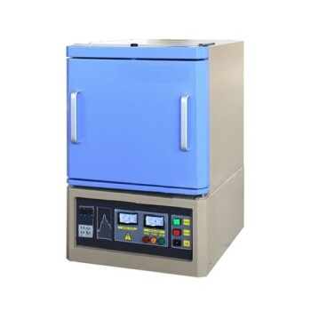
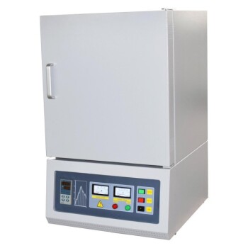
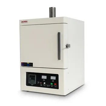
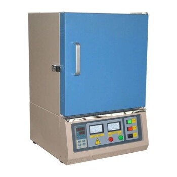
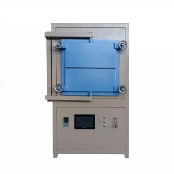
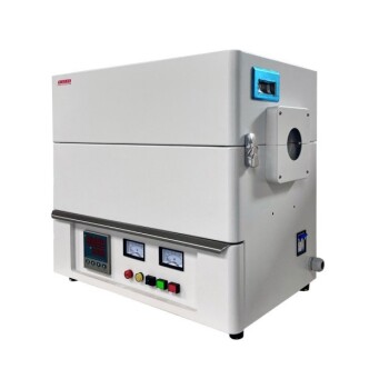
- 1400℃ High Temperature Laboratory Tube Furnace with Alumina Tube
- 1700℃ High Temperature Laboratory Tube Furnace with Alumina Tube
- 1800℃ High Temperature Muffle Oven Furnace for Laboratory
- 1700℃ High Temperature Muffle Oven Furnace for Laboratory
- 1200℃ Muffle Oven Furnace for Laboratory
People Also Ask
- What is a high temperature tube furnace? Achieve Precise Heat and Atmosphere Control
- How do high-temperature laboratory tube furnaces ensure environmental stability? Precision Thermal Reduction Tips
- Why is a high-temperature tube furnace required for NiWO4 calcination? Achieving High-Performance Cathode Materials
- How does a high-temperature tube furnace facilitate sulfur melt-diffusion? Precision Heating for PCFC/S Cathodes
- In what scenarios are laboratory high-temperature tube furnaces or muffle furnaces utilized? Study MgTiO3-CaTiO3 Ceramics