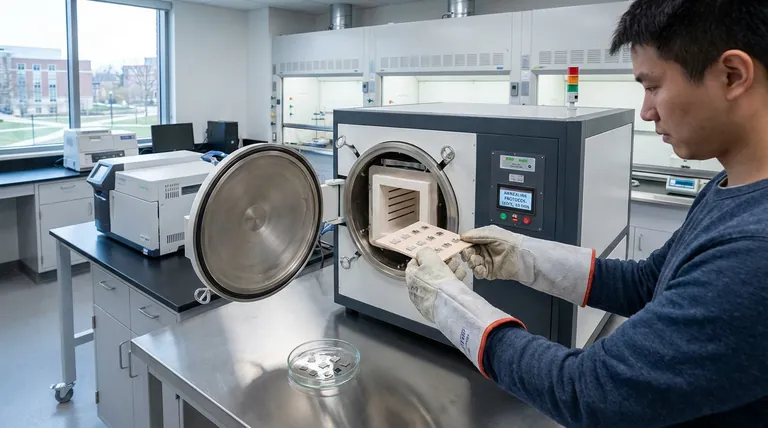
The primary purpose of a final annealing treatment is to physically and electronically integrate the components of an assembled heterojunction device. By subjecting the device to controlled heat—specifically 100°C for 10 minutes—you transform a loose mechanical assembly into a unified electronic system, ensuring optimal performance and durability.
The assembly process places materials next to each other, but annealing bonds them at an atomic level. It is the critical bridge between physical fabrication and reliable electronic functionality, converting potential capacity into actual performance.
Optimizing the Heterojunction Interface
The transfer of materials like FAPbBr3 nanosheets and CdS nanobelts often leaves microscopic imperfections. Annealing addresses the physical limitations of the assembly process.
Achieving Atomic-Level Contact
Simply placing one material atop another does not guarantee a seamless connection. There are often microscopic gaps that impede electron flow.
Heating the device promotes atomic-level close contact at the interface between the semiconductor layers. This physical proximity is essential for the device to function as a cohesive unit rather than two separate layers.
Enhancing Charge Transfer Efficiency
The direct result of tighter atomic contact is improved electronic behavior.
By closing physical gaps, you significantly enhance charge transfer efficiency. This ensures that carriers (electrons and holes) can move freely across the heterojunction without being trapped or scattered at the interface.
Remedying Assembly Defects
The physical act of transferring delicate nanomaterials inevitably introduces structural flaws. Annealing acts as a corrective measure for these fabrication side effects.
Eliminating Mechanical Stress
During the transfer phase, the delicate nanosheets and nanobelts are often stretched or compressed. This creates residual mechanical stress within the lattice.
Annealing provides the thermal energy necessary to relax the material structure. This process eliminates mechanical stress, allowing the crystal lattice to settle into its most energetically favorable state.
Boosting Responsiveness and Stability
A device riddled with internal stress is prone to erratic behavior and premature failure.
By relieving this stress and improving the interface, the treatment significantly improves the responsiveness of the optoelectronic detector. Furthermore, it enhances the device's long-term stability, preventing degradation that can occur over time in stressed materials.
Understanding the Trade-offs
While annealing is beneficial, it requires strict adherence to specific parameters to avoid damaging the sensitive nanomaterials.
Strict Temperature Controls
The process relies on a specific temperature window (100°C). Deviating from this can be detrimental.
Excessive heat could thermally degrade the organic-inorganic hybrid materials (like FAPbBr3), destroying the crystal structure rather than optimizing it.
Time Sensitivity
The duration of the treatment is equally critical. The reference specifies a concise 10-minute window.
Prolonged exposure to heat, even at moderate temperatures, could lead to unwanted material diffusion or oxidation, potentially compromising the sharp interface required for a heterojunction.
Making the Right Choice for Your Goal
To ensure your device meets its performance metrics, consider how this step aligns with your specific objectives.
- If your primary focus is High Sensitivity (Responsiveness): Ensure the annealing reaches the full 100°C to maximize atomic contact, which is the primary driver of efficient charge transfer.
- If your primary focus is Device Longevity (Stability): Do not skip this step, as relieving mechanical stress is the most effective way to prevent physical delamination or electronic drift over time.
By strictly following the 100°C for 10 minutes protocol, you ensure the device is physically relaxed and electronically optimized for peak operation.
Summary Table:
| Parameter/Factor | Impact on Heterojunction Device |
|---|---|
| Temperature (100°C) | Ensures atomic-level contact without degrading sensitive materials. |
| Duration (10 min) | Allows lattice relaxation while preventing unwanted material diffusion. |
| Interface Quality | Converts mechanical assembly into a unified system; boosts charge transfer. |
| Mechanical Stress | Thermal energy eliminates residual stress from the material transfer process. |
| Device Outcome | Significantly improves responsiveness and operational stability. |
Maximize Your Research Precision with KINTEK
Successful heterojunction fabrication depends on precise thermal control. Backed by expert R&D and manufacturing, KINTEK offers high-performance Muffle, Tube, and Vacuum systems, as well as specialized lab high-temp furnaces and heating plates—all customizable to meet your unique semiconductor and nanomaterial needs.
Don't let mechanical stress or poor interface contact compromise your device's responsiveness. Ensure perfect atomic bonding with our reliable thermal solutions.
Ready to elevate your lab's capabilities? Contact KINTEK today for a custom consultation!
Visual Guide

References
- Yao Liu, Yingkai Liu. High-response formamidine bromide lead hybrid cadmium sulfide photodetector. DOI: 10.3788/col202422.022502
This article is also based on technical information from Kintek Furnace Knowledge Base .
Related Products
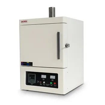
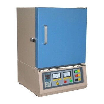
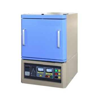
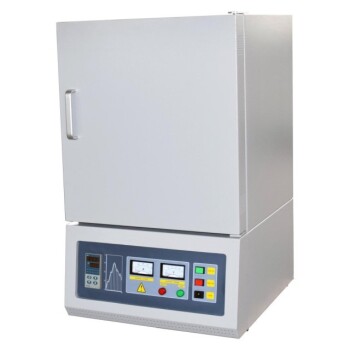
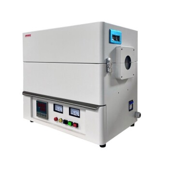
- Laboratory Muffle Oven Furnace with Bottom Lifting
- 1200℃ Muffle Oven Furnace for Laboratory
- 1400℃ Muffle Oven Furnace for Laboratory
- 1800℃ High Temperature Muffle Oven Furnace for Laboratory
- 1700℃ High Temperature Muffle Oven Furnace for Laboratory
People Also Ask
- What is the function of a laboratory muffle furnace in the carbonization process? Transform Waste into Nanosheets
- What critical experimental conditions does a laboratory muffle furnace provide for waste sample oxidation? Achieve Precision
- What role does a muffle furnace play in 600°C carbonization of palm shells? Unlock High-Performance Activated Carbon
- What role does a laboratory muffle furnace play in the ash analysis of plant samples? Achieve Clean Mineral Isolation
- What is the core role of a laboratory muffle furnace in rice husk-based biochar? Master Your Pyrolysis Process