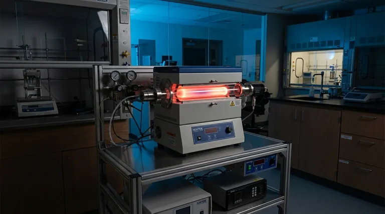
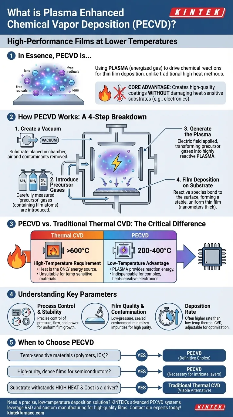
In essence, Plasma Enhanced Chemical Vapor Deposition (PECVD) is a process used to deposit exceptionally thin, high-performance films onto a surface, known as a substrate. Unlike traditional methods that rely solely on intense heat, PECVD uses an energized gas, or plasma, to drive the chemical reactions needed to form the film. This allows the entire process to occur at significantly lower temperatures.
The core advantage of PECVD is its ability to create high-quality coatings without exposing the underlying material to damaging high temperatures. This makes it an essential technology for manufacturing modern electronics and other heat-sensitive components.
How PECVD Works: A Step-by-Step Breakdown
The PECVD process takes place inside a controlled vacuum chamber. While the specific parameters vary by application, the fundamental steps remain consistent.
Step 1: Creating a Vacuum Environment
First, the substrate is placed inside a reaction chamber, and a vacuum is created. This removes air and other potential contaminants, ensuring the purity of the final film.
Step 2: Introducing Precursor Gases
With the vacuum established, carefully measured amounts of one or more "precursor" gases are introduced into the chamber. These gases contain the atoms (like silicon, nitrogen, or carbon) that will eventually form the solid film.
Step 3: Generating the Plasma
This is the key step that defines PECVD. An electric field is applied within the chamber, which energizes the precursor gases and transforms them into a plasma. This plasma is a highly reactive state of matter containing ions and free radicals.
This energy, not extreme heat, breaks down the precursor gas molecules into the reactive components needed for deposition.
Step 4: Film Deposition on the Substrate
The reactive chemical species created in the plasma then diffuse toward the substrate. Upon reaching the surface, they bond to it—and to each other—to form a stable, solid, and uniform thin film, often just nanometers thick.
PECVD vs. Traditional Thermal CVD: The Critical Difference
To fully grasp the value of PECVD, it is crucial to compare it to its predecessor, conventional Chemical Vapor Deposition (CVD).
The High-Temperature Requirement of Thermal CVD
In traditional thermal CVD, heat is the only tool used to initiate the chemical reactions. The substrate must be heated to very high temperatures (often over 600°C) to provide enough energy to break down the precursor gases as they pass over the surface.
This high-heat requirement makes thermal CVD unsuitable for depositing films on materials that have low melting points or are otherwise sensitive to temperature, such as many polymers or completed electronic circuits.
The Low-Temperature Advantage of PECVD
PECVD circumvents this limitation. By using plasma to break down the precursor gases, the substrate itself does not need to be super-heated. The plasma provides the necessary energy for the reaction, allowing deposition to occur at much lower temperatures (typically 200-400°C).
This low-temperature capability is the primary reason PECVD is indispensable in the semiconductor industry for building complex, multi-layered microchips.
Understanding the Trade-offs and Key Parameters
While powerful, PECVD is a sophisticated process that requires precise control to achieve the desired results.
Process Control and Stability
Achieving a stable plasma is critical for uniform film growth. This requires precise control over chamber pressure, gas flow rates, and the power supplied to generate the plasma. Modern systems are highly automated to manage these variables.
Film Quality and Contamination
Because the process occurs in a sealed, low-pressure environment, the risk of atmospheric contamination is very low. High-quality reactor designs, often using metal chambers, further minimize the introduction of impurities, leading to higher-purity films.
Deposition Rate
The use of plasma often allows for a higher deposition rate compared to low-temperature thermal CVD processes. The working pressure can be adjusted to optimize the growth rate of the film without sacrificing quality.
When to Choose PECVD
Selecting the right deposition method depends entirely on the requirements of your substrate and the desired properties of the final film.
- If your primary focus is depositing films on temperature-sensitive materials: PECVD is the definitive choice, as its low-temperature process prevents damage to plastics, polymers, or complex integrated circuits.
- If your primary focus is creating high-purity, dense films for semiconductors: PECVD provides the control and low-temperature environment necessary for building the intricate layers of modern electronic devices.
- If your substrate can withstand high heat and cost is a major driver: Traditional thermal CVD may be a viable alternative, as the equipment can be less complex than a full PECVD system.
Ultimately, understanding the trade-off between thermal energy and plasma energy is the key to selecting the right deposition strategy for your application.
Summary Table:
| Feature | PECVD | Traditional Thermal CVD |
|---|---|---|
| Process Temperature | Low (200-400°C) | High (Often >600°C) |
| Primary Energy Source | Plasma (Electric Field) | Thermal (Heat) |
| Ideal For | Temperature-sensitive substrates (e.g., polymers, ICs) | High-temperature tolerant substrates |
| Key Advantage | Prevents thermal damage to sensitive materials | Simpler system design (for high-temp applications) |
Need a precise, low-temperature deposition solution for your sensitive materials?
KINTEK's advanced PECVD systems leverage our exceptional R&D and in-house manufacturing to deliver the high-quality, uniform thin films your laboratory requires. Our deep customization capabilities ensure the system is tailored to your unique experimental parameters.
Let's discuss how our PECVD technology can enhance your research and development. Contact our experts today for a consultation.
Visual Guide
Related Products
- RF PECVD System Radio Frequency Plasma Enhanced Chemical Vapor Deposition
- Slide PECVD Tube Furnace with Liquid Gasifier PECVD Machine
- Inclined Rotary Plasma Enhanced Chemical Deposition PECVD Tube Furnace Machine
- Inclined Rotary Plasma Enhanced Chemical Deposition PECVD Tube Furnace Machine
- MPCVD Machine System Reactor Bell-jar Resonator for Lab and Diamond Growth
People Also Ask
- What are the limitations of PECVD? Overcome Process Control and Cost Challenges
- What are the system specifications of the PECVD system? Unlock Precision Thin-Film Deposition
- What are the key advantages of PECVD technology? Achieve Low-Temperature, High-Quality Thin Film Deposition
- What are some promising applications of PECVD-prepared 2D materials? Unlock Advanced Sensing and Optoelectronics
- What is the role of RF power in PECVD and how does the RF-PECVD process work? Master Thin Film Deposition Control


