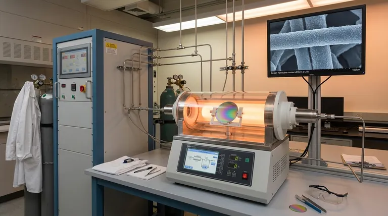
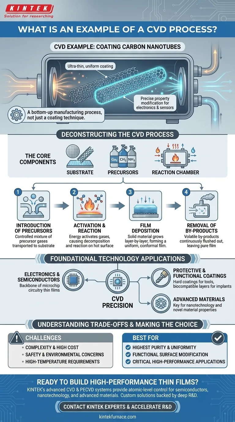
As a specific example, Chemical Vapor Deposition (CVD) is used to apply an ultra-thin, uniform coating onto carbon nanotubes. These tiny cylinders of carbon can have their mechanical or chemical properties precisely modified by the deposited film, enabling them to be used in advanced electronics or as specialized chemical sensors. This process exemplifies how CVD can build functional layers on complex, microscopic structures.
CVD is not simply a coating technique; it is a bottom-up manufacturing process. It involves constructing a solid, high-performance thin film directly onto a substrate by engineering chemical reactions from a gas phase, offering atomic-level control over the final material.
Deconstructing the CVD Process
To understand any CVD example, you must first understand the fundamental steps and components. The process, while complex in practice, is elegant in its core concept. It consistently involves a substrate, chemical precursors, and a controlled environment.
The Core Components
The process begins with three key elements:
- The Substrate: This is the material or object to be coated, such as a silicon wafer, a medical implant, or the carbon nanotubes from our example.
- The Precursors: These are volatile gases or vaporized liquids that contain the atoms needed to build the desired film. Their selection is critical to the final film's properties.
- The Reaction Chamber: A sealed chamber that contains the substrate and allows for precise control of temperature, pressure, and gas flow.
Step 1: Introduction of Precursors
The process is initiated by feeding a carefully controlled mixture of precursor gases into the reaction chamber. These gases are transported toward the substrate, often with the help of an inert carrier gas.
Step 2: Activation and Reaction
Energy, typically in the form of high heat, is applied to the chamber. This energy "activates" the precursor gases, causing them to decompose and react on or near the hot substrate surface. This is the crucial chemical transformation step.
Step 3: Film Deposition
As the precursors react, they form a solid material that deposits onto the substrate surface. This film grows layer by layer, sometimes atom by atom, resulting in a highly uniform and dense coating that conforms perfectly to the substrate's shape.
Step 4: Removal of By-products
The chemical reactions also produce unwanted volatile by-products. These waste gases are continuously flushed out of the reaction chamber by the gas flow, leaving only the desired solid film behind.
Why CVD is a Foundational Technology
The precision of CVD makes it indispensable across numerous high-tech industries. It is not used for simple coatings but for creating materials with specific, engineered functions.
In Electronics and Semiconductors
CVD is the backbone of the semiconductor industry. It is used to deposit the various insulating, conducting, and semiconducting thin films that form the intricate circuitry of microchips.
For Protective and Functional Coatings
The process is used to apply extremely hard coatings to machine tools, increasing their lifespan and performance. It's also used to create biocompatible coatings on medical implants or corrosion-resistant layers in harsh environments.
In Advanced Materials
As seen in the nanotube example, CVD is a key tool in nanotechnology and materials science. It allows researchers to create novel materials and surfaces with unique optical, electrical, or mechanical properties.
Understanding the Trade-offs
While powerful, CVD is not a universal solution. Its implementation requires careful consideration of its inherent complexities and limitations.
Complexity and High Cost
CVD systems are sophisticated and expensive pieces of equipment. The process requires precise control over multiple variables (temperature, pressure, gas flows), demanding significant expertise to operate correctly.
Safety and Environmental Concerns
Many precursor gases used in CVD are highly toxic, flammable, or corrosive. The process also generates hazardous waste by-products that require specialized handling, ventilation, and disposal protocols to ensure operator safety and mitigate environmental impact.
High-Temperature Requirements
Traditional thermal CVD often requires very high temperatures. This can limit the types of substrate materials that can be used, as many materials cannot withstand the heat without deforming or melting.
Making the Right Choice for Your Goal
Your decision to consider CVD should be based on your primary technical objective. The process is best suited for applications where material performance is paramount.
- If your primary focus is to achieve the highest purity and uniformity: CVD is an exceptional choice for applications like microelectronics, where flawless, dense films are non-negotiable.
- If your primary focus is to functionally modify a material's surface: CVD provides a way to add new properties, such as wear resistance or chemical reactivity, without altering the bulk of the substrate.
- If your primary focus is exploring manufacturing options for a new product: View CVD as a high-performance, high-cost option that is justified when the properties of the thin film are critical to your product's function.
Ultimately, understanding CVD is understanding how the foundational materials of modern technology are built from the atoms up.
Summary Table:
| CVD Process Stage | Key Action | Outcome |
|---|---|---|
| 1. Introduction | Precursor gases enter the chamber | Gases are transported to the substrate surface |
| 2. Activation | Energy (heat) triggers chemical reactions | Precursors decompose on the hot substrate |
| 3. Deposition | Solid material forms layer-by-layer | A uniform, conformal thin film is created |
| 4. By-product Removal | Waste gases are flushed from the chamber | Pure, high-performance coating remains |
Ready to build high-performance thin films with precision?
KINTEK's advanced CVD and PECVD systems, backed by our deep R&D and in-house manufacturing expertise, provide the atomic-level control and uniformity required for cutting-edge applications in semiconductors, nanotechnology, and advanced materials.
Our team works with you to customize a furnace solution—whether it's a Tube Furnace, Vacuum & Atmosphere Furnace, or a specialized CVD/PECVD System—that perfectly matches your unique process requirements.
Contact our experts today to discuss how our CVD technology can accelerate your research and development.
Visual Guide
Related Products
- Custom Made Versatile CVD Tube Furnace Chemical Vapor Deposition CVD Equipment Machine
- Split Chamber CVD Tube Furnace with Vacuum Station CVD Machine
- Multi Heating Zones CVD Tube Furnace Machine for Chemical Vapor Deposition Equipment
- Slide PECVD Tube Furnace with Liquid Gasifier PECVD Machine
- Controlled Inert Nitrogen Hydrogen Atmosphere Furnace
People Also Ask
- Why are CVD tube furnace sintering systems indispensable for 2D material research and production? Unlock Atomic-Scale Precision
- What is the working principle of a CVD tube furnace? Achieve Precise Thin Film Deposition for Your Lab
- How might AI and machine learning enhance CVD tube furnace processes? Boost Quality, Speed, and Safety
- How does CVD tube furnace sintering enhance graphene growth? Achieve Superior Crystallinity and High Electron Mobility
- How can integrating CVD tube furnaces with other technologies benefit device fabrication? Unlock Advanced Hybrid Processes


