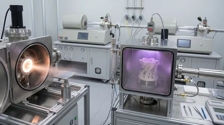
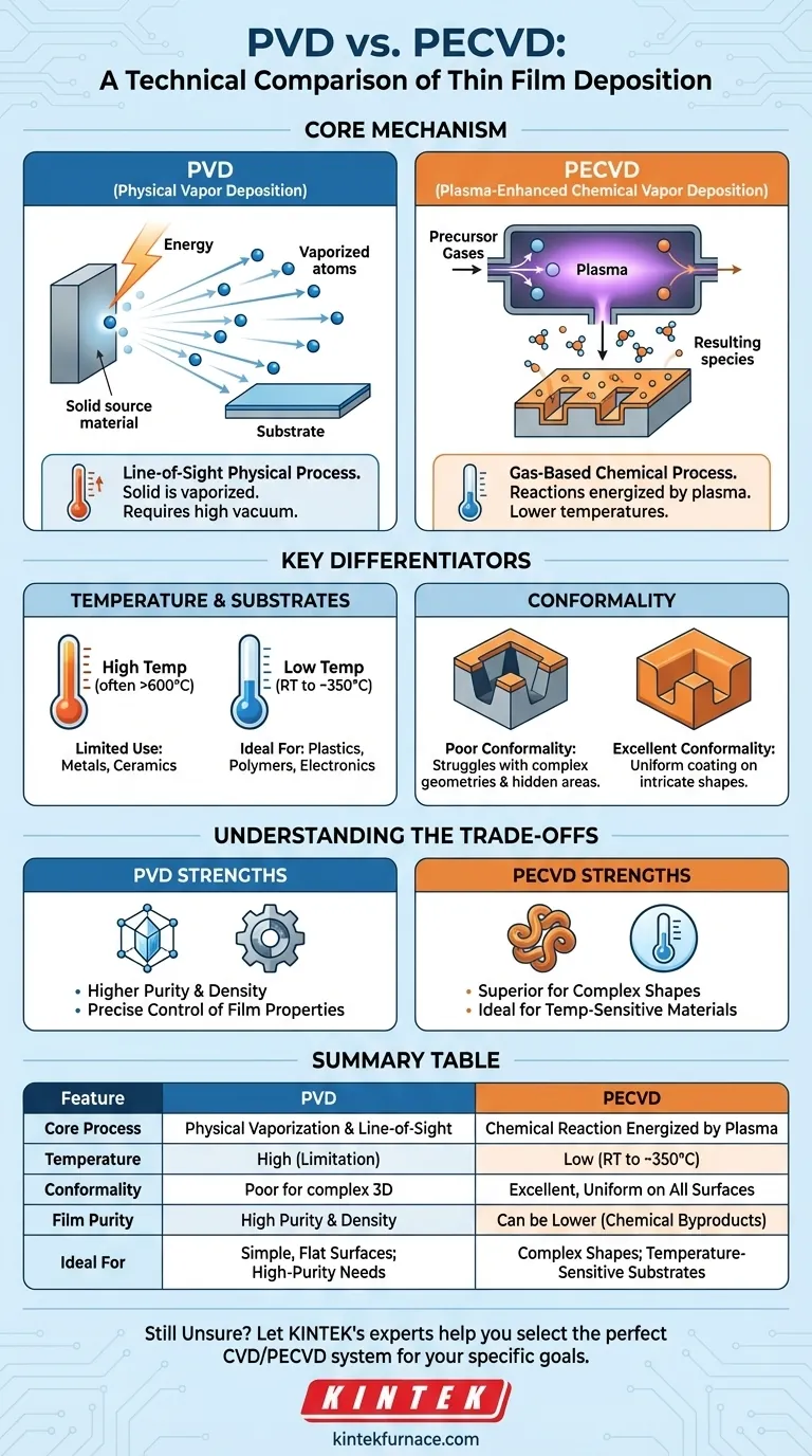
The fundamental difference between PVD and PECVD lies in how the coating material is delivered to a surface. Physical Vapor Deposition (PVD) is a "line-of-sight" mechanical process where a solid material is vaporized and physically travels to coat a substrate. In contrast, Plasma-Enhanced Chemical Vapor Deposition (PECVD) is a chemical process where gases react and form a solid film on the substrate, with the reactions energized by plasma instead of high heat.
Choosing between PVD and PECVD is a decision driven by two critical factors: the complexity of your substrate's geometry and its tolerance for heat. PVD offers high purity via a direct line-of-sight method, while PECVD provides uniform coverage on complex shapes at low temperatures.
The Core Mechanism: Physical vs. Chemical
To understand the practical differences, you must first grasp the foundational principles. PVD and PECVD belong to two different families of deposition technology.
### Physical Vapor Deposition (PVD): A Line-of-Sight Process
PVD is fundamentally a physical process. Think of it as an atomic-scale spray-painting operation that takes place in a vacuum.
A solid source material is bombarded with energy (like an ion beam or electron beam) until its atoms are vaporized. These vaporized atoms then travel in a straight line through the vacuum and condense onto the substrate, forming a thin film.
Because the particles travel in a straight line, any part of the substrate not in the direct "line of sight" of the source material will not get coated, or will receive a much thinner coating.
### Plasma-Enhanced Chemical Vapor Deposition (PECVD): A Gas-Based Process
PECVD is a type of Chemical Vapor Deposition (CVD). Instead of a solid source, it begins with precursor gases introduced into a chamber.
The key innovation is the use of plasma, an energized state of gas. The plasma provides the energy needed to break down the precursor gases and drive the chemical reactions that form the thin film, all without requiring extreme heat.
This process is diffusive, like a chemical fog that settles and reacts on all exposed surfaces. The plasma and reactive gases can surround the object, allowing for a highly uniform coating.
Key Differentiators in Practice
The differences in their core mechanisms lead to critical distinctions in how they are applied and what results they produce.
### Temperature: The Decisive Factor for Substrates
Traditional CVD requires very high temperatures (often 600–800°C) to provide the thermal energy for chemical reactions to occur. This limits its use to materials that can withstand extreme heat.
PECVD solves this problem by using plasma energy instead of thermal energy. This allows for deposition at much lower temperatures, from room temperature up to around 350°C.
This low-temperature capability makes PECVD ideal for coating temperature-sensitive substrates like plastics, polymers, or electronic components that would be damaged or destroyed by high heat.
### Conformality: Coating Complex Geometries
Conformality refers to a coating's ability to maintain a uniform thickness over a complex, non-flat surface. This is where the two methods diverge significantly.
PVD's line-of-sight nature makes it struggle with complex geometries. Surfaces inside trenches, around sharp corners, or on the "back side" of a part will receive little to no coating.
PECVD excels at conformality. Because it is a gas-driven process, the reactive chemical species can diffuse into and around intricate features, ensuring a highly uniform and consistent film thickness on all surfaces.
Understanding the Trade-offs
Neither technology is universally superior; the optimal choice depends on the specific requirements of the application.
### Film Purity and Density
PVD generally produces films with higher purity and density. Since the source material is physically transferred to the substrate without chemical reactions, there are fewer opportunities for impurities or chemical byproducts to be incorporated into the film.
PECVD, being a chemical process, can sometimes result in lower-purity films. Incomplete reactions or byproducts from the precursor gases can become trapped in the growing film.
### Process Control and Film Properties
PVD offers very precise control over film properties like grain structure and stoichiometry, as the process is physically direct and easier to model. This makes it a preferred method for applications like optical coatings or semiconductors where exact material properties are critical.
PECVD process control involves balancing gas flow rates, pressure, and plasma power, which can be more complex. However, this complexity also allows for the creation of unique film chemistries that are not possible with PVD.
Making the Right Choice for Your Application
Your decision should be guided by your primary technical goal.
- If your primary focus is coating a simple, flat surface with the highest possible purity: PVD is almost always the superior choice due to its direct deposition mechanism and low impurity levels.
- If your primary focus is uniformly coating a complex, 3D part: PECVD is the clear winner because its gas-based nature provides excellent conformality that PVD cannot match.
- If your primary focus is coating a temperature-sensitive material like plastic: PECVD is the necessary choice, as its low-temperature process prevents damage to the substrate.
By understanding the fundamental trade-off between PVD's physical line-of-sight and PECVD's chemical conformal coating, you can confidently select the right technology for your specific engineering challenge.
Summary Table:
| Feature | PVD (Physical Vapor Deposition) | PECVD (Plasma-Enhanced Chemical Vapor Deposition) |
|---|---|---|
| Core Process | Physical vaporization & line-of-sight transfer | Chemical reaction of gases energized by plasma |
| Temperature | High (can be a limitation) | Low (room temp to ~350°C) |
| Conformality | Poor for complex, 3D geometries | Excellent, uniform coating on all surfaces |
| Film Purity | High purity and density | Can be lower due to chemical byproducts |
| Ideal For | Simple geometries, high-purity needs | Complex shapes, temperature-sensitive substrates |
Still Unsure Which Coating Technology is Right for Your Project?
Leveraging exceptional R&D and in-house manufacturing, KINTEK provides diverse laboratories with advanced high-temperature furnace solutions. Our product line, including Muffle, Tube, Rotary Furnaces, Vacuum & Atmosphere Furnaces, and CVD/PECVD Systems, is complemented by our strong deep customization capability to precisely meet unique experimental requirements.
Let our experts help you select the perfect system to achieve your specific coating goals. Contact us today for a personalized consultation!
Visual Guide
Related Products
- RF PECVD System Radio Frequency Plasma Enhanced Chemical Vapor Deposition
- Inclined Rotary Plasma Enhanced Chemical Deposition PECVD Tube Furnace Machine
- Slide PECVD Tube Furnace with Liquid Gasifier PECVD Machine
- HFCVD Machine System Equipment for Drawing Die Nano Diamond Coating
- Inclined Rotary Plasma Enhanced Chemical Deposition PECVD Tube Furnace Machine
People Also Ask
- How are deposition rates and film properties controlled in PECVD? Master Key Parameters for Optimal Thin Films
- What is RF in PECVD? A Critical Control for Plasma Deposition
- What are some promising applications of PECVD-prepared 2D materials? Unlock Advanced Sensing and Optoelectronics
- What are the applications of plasma enhanced chemical vapor deposition? Key Uses in Electronics, Optics & Materials
- What are the key advantages of PECVD technology? Achieve Low-Temperature, High-Quality Thin Film Deposition


