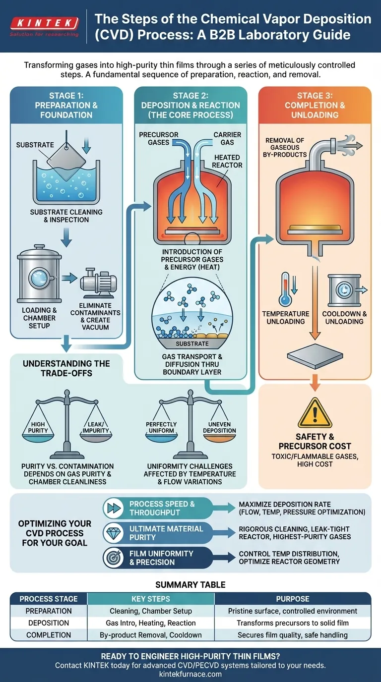
At its core, the Chemical Vapor Deposition (CVD) process is a series of meticulously controlled steps that transform gases into a solid, high-purity thin film on a target object. The fundamental sequence involves preparing a substrate, introducing reactive precursor gases into a heated chamber, inducing a chemical reaction that deposits a solid material onto the substrate, and removing the gaseous by-products.
The core principle of CVD is not just about coating a surface; it's about precisely engineering a material from the ground up, one molecular layer at a time. Understanding each step is to understand how to control the final properties of the deposited film.
The Foundational Stage: Preparation
Before any deposition can occur, the environment and the substrate must be perfectly prepared. This stage sets the foundation for the adhesion and quality of the final film.
Substrate Cleaning and Inspection
The first step is a rigorous cleaning of the substrate, which is the material to be coated. Any contaminants, such as oils or microscopic dust, will prevent the film from adhering properly and can introduce impurities. This often involves chemical baths and inspection to ensure a pristine surface.
Loading and Chamber Setup
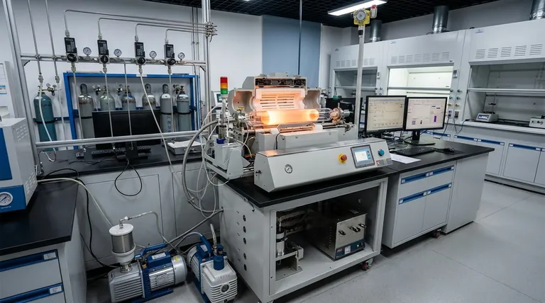
The cleaned substrate is placed inside the CVD reactor, which is a highly controlled chamber. The chamber is sealed and purged, often creating a vacuum or a specific atmospheric condition, to eliminate unwanted reactive particles like oxygen.
The Heart of the Process: Gas Reaction and Deposition
This is where the transformation from gas to solid occurs. It is a delicate balance of transport phenomena and chemical reactions controlled by temperature, pressure, and gas flow.
Introduction of Precursor Gases
Specific gases, known as precursors, are introduced into the reactor at a controlled flow rate. These are molecules that contain the atoms desired in the final film. They are often mixed with a carrier gas (like argon or hydrogen) which helps transport the precursors to the substrate.
The Role of Energy
The reactor is heated to precise, often very high, temperatures. This thermal energy provides the activation energy needed to break the chemical bonds within the precursor molecules, making them reactive.
Gas Transport to the Substrate
The precursor gases flow toward the substrate. Directly above the substrate surface exists a thin, static layer of gas known as the boundary layer. The reactive species must diffuse through this layer to reach the surface.
Adsorption and Surface Reaction
Once the reactive species reach the substrate, they stick to the surface in a process called adsorption. The hot surface itself often acts as a catalyst, driving the final chemical reaction that forms the solid film and releases volatile by-products.
The Result: Film Growth and Process Completion
The successful reaction results in the formation of a solid film. The process concludes with steps to ensure the film's stability and safe removal of the coated part.
Building the Film, Layer by Layer
The solid material from the surface reaction builds up, forming a thin, dense, and uniform film. The thickness of this film is precisely controlled by managing the deposition time, temperature, and gas flow rates.
Removal of Gaseous By-products
The chemical reactions create desired solids but also unwanted gaseous by-products. These must be continuously exhausted from the chamber to prevent them from contaminating the film or interfering with the deposition process.
Cooldown and Unloading
After the desired thickness is achieved, the gas flow is stopped and the reactor is safely cooled down. Once at a safe temperature, the chamber is purged with an inert gas and brought back to atmospheric pressure, allowing the newly coated substrate to be unloaded.
Understanding the Trade-offs
While powerful, the CVD process is not without its challenges. Success depends on navigating a complex interplay of variables where small deviations can have significant impacts.
Purity vs. Contamination
The high quality of a CVD film is entirely dependent on the purity of the precursor gases and the cleanliness of the chamber. Even a microscopic leak in the system can introduce oxygen or water vapor, leading to a contaminated and defective film.
Uniformity Challenges
Achieving a perfectly uniform film thickness across a large or complex-shaped substrate is difficult. Variations in temperature or gas flow across the substrate can lead to uneven deposition rates, impacting the performance of the final part.
Safety and Precursor Cost
Many precursor gases used in CVD are highly toxic, flammable, or corrosive, requiring extensive safety protocols and handling systems. Furthermore, high-purity precursors can be extremely expensive, making it a significant cost factor in production.
Making the Right Choice for Your Goal
Your primary objective determines which steps of the CVD process demand the most attention.
- If your primary focus is process speed and throughput: Optimizing the gas flow rates, temperature, and pressure to maximize the deposition rate without sacrificing basic uniformity is your key challenge.
- If your primary focus is ultimate material purity: Your efforts should be concentrated on rigorous substrate cleaning, ensuring a leak-tight reactor, and using the highest-purity precursor and carrier gases available.
- If your primary focus is film uniformity and precision: Controlling the temperature distribution across the substrate and optimizing the reactor geometry to manage gas flow dynamics are the most critical factors.
Ultimately, mastering CVD is about controlling a cascade of physical and chemical events to build a material with intention.
Summary Table:
| Process Stage | Key Steps | Purpose |
|---|---|---|
| Preparation | Substrate Cleaning, Chamber Setup | Ensures a pristine surface and controlled environment for deposition. |
| Deposition | Gas Introduction, Heating, Surface Reaction | Transforms precursor gases into a solid film on the substrate. |
| Completion | By-product Removal, Cooldown, Unloading | Secures the final film quality and allows for safe part handling. |
Ready to engineer high-purity thin films with precision? The CVD process demands exact control over every stage, from precursor gas handling to temperature management. At KINTEK, we leverage our exceptional R&D and in-house manufacturing to provide advanced CVD/PECVD systems tailored to your unique experimental requirements. Whether you need to optimize for speed, purity, or uniformity, our deep customization capabilities ensure your furnace solution meets the challenge. Contact us today to discuss how our expertise can enhance your laboratory's capabilities. Get in touch via our contact form
Visual Guide
Related Products
- HFCVD Machine System Equipment for Drawing Die Nano Diamond Coating
- Custom Made Versatile CVD Tube Furnace Chemical Vapor Deposition CVD Equipment Machine
- Cylindrical Resonator MPCVD Machine System for Lab Diamond Growth
- Multi Heating Zones CVD Tube Furnace Machine for Chemical Vapor Deposition Equipment
- 915MHz MPCVD Diamond Machine Microwave Plasma Chemical Vapor Deposition System Reactor
People Also Ask
- How can customers maximize the quality of CVD coatings? Master Pre-Coating Prep for Superior Results
- What materials are commonly used in CVD coating systems? Explore Key Materials for Superior Coatings
- What are the equipment for chemical vapor deposition? A Guide to the 5 Essential Components
- What is chemical vapor deposition (CVD) and its primary industrial application? Unlock Precision Thin Films for Electronics
- What is the function of high-purity Argon (Ar) gas during CVD? Optimize Your Thin Film Uniformity and Purity


