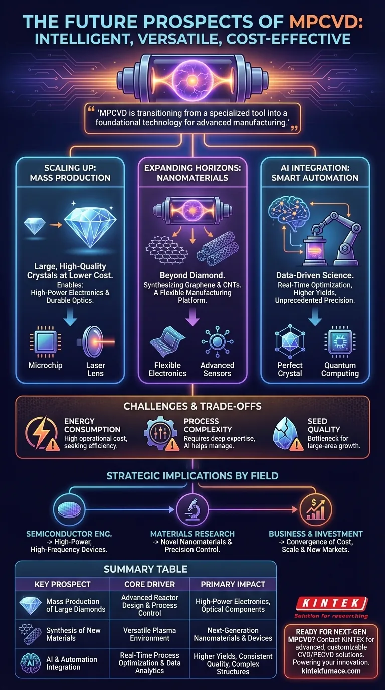
The future of MPCVD is exceptionally strong, driven by its evolution into an intelligent, versatile, and cost-effective platform for creating advanced materials. Its prospects lie in three key areas: the mass production of large, high-quality diamond crystals for next-generation electronics; the expansion into synthesizing other nanomaterials like graphene; and the integration of AI to automate and perfect the manufacturing process.
MPCVD is transitioning from a specialized tool for diamond synthesis into a foundational technology for advanced manufacturing. Its future is defined not just by making better materials, but by making them at a scale and cost that unlocks entirely new applications in electronics, optics, and materials science.
The Path to Mainstream Adoption
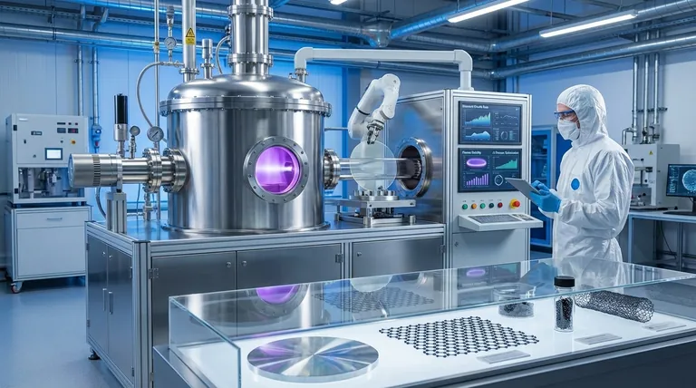
Microwave Plasma Chemical Vapor Deposition (MPCVD) is moving beyond its traditional role. The core trends are not isolated improvements but interconnected developments pushing the technology toward broader industrial and scientific relevance.
Scaling Up: The Pursuit of Large, High-Quality Crystals
The most immediate and impactful trend is the push for mass production of large-scale, single-crystal diamonds. For decades, this was the "holy grail" of materials science.
Advances in reactor design, seed crystal quality, and synthesis recipes are converging. This allows for the growth of larger, purer crystals at a faster rate and a significantly lower cost than ever before.
This scaling is critical for applications like high-power electronic devices and durable optical components, which require wafer-sized diamond substrates that were previously economically unfeasible.
Expanding the Material Palette: Beyond Diamond
While diamond synthesis remains the flagship application, the fundamental principles of MPCVD are being applied to a wider range of advanced materials.
The controlled plasma environment is ideal for depositing nanomaterials like graphene and carbon nanotubes (CNTs) with high precision.
This versatility transforms MPCVD from a single-purpose tool into a flexible manufacturing platform capable of producing the foundational materials for different next-generation technologies.
The Integration of Intelligence and Automation
The next leap for MPCVD involves making the process smarter. Historically, achieving high-quality results required deep operator expertise and manual process control, which limited scalability and repeatability.
From Manual Tweaking to AI-Driven Optimization
Modern MPCVD systems are beginning to integrate automation and artificial intelligence. AI algorithms can monitor the plasma in real-time, analyzing data from sensors to make micro-adjustments to gas flow, pressure, and microwave power.
This moves the process from a manually-intensive art to a data-driven science, ensuring higher yields and consistent quality across production runs.
Enabling Unprecedented Precision
For complex structures like semiconductor devices, precision is everything. AI-driven process control allows for the execution of highly complex, multi-stage growth recipes that would be nearly impossible to manage manually.
This level of control is essential for creating the defect-free layers required for diamond electronics and quantum sensing applications.
Understanding the Challenges and Trade-offs
To fully appreciate its future, we must also acknowledge the hurdles that MPCVD technology is actively working to overcome.
The Energy Consumption Dilemma
MPCVD reactors require substantial energy to generate and sustain the high-density plasma needed for material growth. While newer systems are becoming more energy-efficient, power consumption remains a significant operational cost.
This is a critical factor for mass production, as energy costs directly impact the final price point of the synthesized material.
Complexity of Process Control
The sheer number of variables—gas mixture, temperature, pressure, microwave power—makes the MPCVD process inherently complex. Achieving the desired material properties requires a deep understanding of plasma physics and chemistry.
While AI helps manage this complexity, developing the initial process "recipe" for a new material or quality standard remains a highly specialized and time-consuming task.
Dependence on Seed Quality
The quality of the final crystal is fundamentally limited by the quality of the initial seed material it grows upon. Sourcing or producing large, defect-free seed crystals is a critical bottleneck for scaling up production of large-area single-crystal diamonds.
Making the Right Choice for Your Goal
Understanding these trends allows you to see how MPCVD might impact your specific field.
- If your primary focus is semiconductor engineering: The most important trend is the move toward mass-produced, large-area diamond wafers, which will enable high-power, high-frequency electronic devices that surpass the limits of silicon.
- If your primary focus is materials research: The key development is MPCVD's flexibility for synthesizing novel materials like graphene and CNTs, along with the precision afforded by AI-driven process control.
- If your primary focus is business or investment: The critical takeaway is the convergence of lower costs, mass production, and new applications, signaling that MPCVD is opening up significant new markets beyond its traditional industrial uses.
MPCVD is rapidly maturing into a cornerstone technology poised to manufacture the essential materials of the future.
Summary Table:
| Key Future Prospect | Core Driver | Primary Application Impact |
|---|---|---|
| Mass Production of Large Diamonds | Advanced Reactor Design & Process Control | High-Power Electronics, Optical Components |
| Synthesis of New Materials (Graphene, CNTs) | Versatile Plasma Environment | Next-Generation Nanomaterials & Devices |
| AI & Automation Integration | Real-Time Process Optimization & Data Analytics | Higher Yields, Consistent Quality, Complex Structures |
Ready to integrate next-generation MPCVD technology into your research or production line? KINTEK's advanced high-temperature furnace solutions, including our specialized CVD/PECVD systems, are engineered to meet the demanding requirements of modern materials science. Leveraging our exceptional R&D and in-house manufacturing capabilities, we provide robust platforms capable of handling the complex processes detailed above. Our strong deep customization capability ensures your system is precisely tailored to your unique experimental goals, whether you are scaling up diamond synthesis or exploring novel nanomaterials. Contact our experts today to discuss how we can power your innovation.
Visual Guide
Related Products
- 915MHz MPCVD Diamond Machine Microwave Plasma Chemical Vapor Deposition System Reactor
- MPCVD Machine System Reactor Bell-jar Resonator for Lab and Diamond Growth
- Cylindrical Resonator MPCVD Machine System for Lab Diamond Growth
- Multi Heating Zones CVD Tube Furnace Machine for Chemical Vapor Deposition Equipment
- Inclined Rotary Plasma Enhanced Chemical Deposition PECVD Tube Furnace Machine
People Also Ask
- What is the purpose of a microwave plasma chemical vapor deposition system? Grow High-Purity Diamonds and Advanced Materials
- What factors influence the quality of diamond deposition in the MPCVD method? Master the Critical Parameters for High-Quality Diamond Growth
- What are the essential components of an MPCVD reactor system? Build a Pristine Environment for High-Purity Materials
- What are the main components of an MPCVD machine? Unlock the Secrets of Diamond Synthesis
- In which industries is the microwave plasma chemical vapor deposition system commonly used? Unlock High-Purity Material Synthesis


