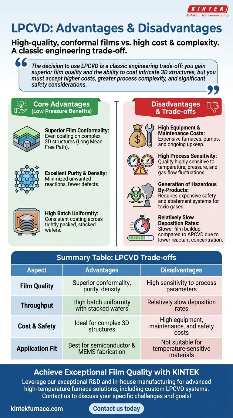
In essence, Low-Pressure Chemical Vapor Deposition (LPCVD) is a process favored for its ability to produce exceptionally high-quality, pure, and uniform thin films that conform perfectly to complex surfaces. This performance, however, comes at the cost of high equipment expense, slower deposition rates, and a process that is highly sensitive to operational parameters.
The decision to use LPCVD is a classic engineering trade-off: you gain superior film quality and the ability to coat intricate 3D structures, but you must accept higher costs, greater process complexity, and significant safety considerations.
The Core Advantages of Operating at Low Pressure
Operating in a vacuum environment fundamentally changes the behavior of precursor gases, which is the source of LPCVD's primary benefits. This makes it a cornerstone technology in semiconductor and MEMS fabrication.
Superior Film Conformality
At low pressure, gas molecules have a long mean free path, meaning they can travel further without colliding with each other. This allows them to reach and deposit evenly on all surfaces of a complex, three-dimensional structure, resulting in a highly conformal coating.
Excellent Purity and Density
The vacuum environment minimizes unwanted gas-phase reactions. Deposition occurs primarily on the substrate surface, leading to denser, purer films with fewer defects and impurities compared to atmospheric pressure methods.
High Batch Uniformity
The process allows for wafers to be stacked vertically and packed tightly together in the furnace. The excellent gas transport at low pressure ensures that all wafers in the batch receive a uniform coating, enabling high-throughput manufacturing with consistent results.
Understanding the Disadvantages and Trade-offs
While powerful, LPCVD is not a universally ideal solution. Its disadvantages are significant and directly related to the equipment and precision required to maintain a low-pressure, high-temperature environment.
High Equipment and Maintenance Costs
LPCVD systems require expensive high-temperature furnaces, sophisticated vacuum pumps, and precise gas flow controllers. The setup and ongoing maintenance of this equipment represent a substantial financial investment.
High Process Sensitivity
The quality of the final film is extremely sensitive to minor fluctuations in temperature, pressure, and gas flow rates. A small deviation can compromise an entire batch, demanding robust process control and monitoring systems.
Generation of Hazardous By-Products
Many precursor gases used in LPCVD are toxic, flammable, or corrosive. Furthermore, the chemical reactions can produce hazardous by-products that must be safely handled and neutralized, requiring expensive exhaust and abatement systems.
Relatively Slow Deposition Rates
A common trade-off for the high film quality is a slower deposition rate compared to atmospheric pressure CVD (APCVD). The lower concentration of reactant species in the chamber means the film builds up more slowly, which can impact overall production throughput.
Making the Right Choice for Your Application
Selecting the right deposition method requires aligning the process capabilities with your primary technical and business goals.
- If your primary focus is maximum film quality and conformality: LPCVD is the superior choice for applications like advanced microelectronics or MEMS where coating intricate features is critical.
- If your primary focus is lower cost and high-volume throughput: Consider alternatives like APCVD if the absolute highest film purity and conformality are not strict requirements.
- If your primary focus is depositing on temperature-sensitive materials: LPCVD's high process temperatures make it unsuitable; Plasma-Enhanced CVD (PECVD) is the standard alternative for lower-temperature deposition.
Ultimately, choosing LPCVD is an investment in achieving the highest possible film quality and uniformity.
Summary Table:
| Aspect | Advantages of LPCVD | Disadvantages of LPCVD |
|---|---|---|
| Film Quality | Superior conformality, purity, and density | High sensitivity to process parameters |
| Throughput | High batch uniformity with stacked wafers | Relatively slow deposition rates |
| Cost & Safety | Ideal for complex 3D structures | High equipment, maintenance, and safety costs |
| Application Fit | Best for semiconductor and MEMS fabrication | Not suitable for temperature-sensitive materials |
Need to achieve exceptional film quality and conformality for your advanced research or production?
At KINTEK, we leverage our exceptional R&D and in-house manufacturing capabilities to provide advanced high-temperature furnace solutions, including custom LPCVD systems. Our product line, featuring Tube Furnaces, Vacuum & Atmosphere Furnaces, and CVD/PECVD Systems, is complemented by strong deep customization capabilities to precisely meet your unique experimental and production requirements.
Let our experts help you determine if LPCVD is the right choice for your application and design a system that delivers the superior performance you need. Contact us today to discuss your specific challenges and goals!
Visual Guide
Related Products
- RF PECVD System Radio Frequency Plasma Enhanced Chemical Vapor Deposition
- Inclined Rotary Plasma Enhanced Chemical Deposition PECVD Tube Furnace Machine
- Inclined Rotary Plasma Enhanced Chemical Deposition PECVD Tube Furnace Machine
- Multi Heating Zones CVD Tube Furnace Machine for Chemical Vapor Deposition Equipment
- Slide PECVD Tube Furnace with Liquid Gasifier PECVD Machine
People Also Ask
- How does film quality compare between PECVD and CVD? Choose the Best Method for Your Substrate
- What is RF in PECVD? A Critical Control for Plasma Deposition
- What is PECVD specification? A Guide to Choosing the Right System for Your Lab
- How are deposition rates and film properties controlled in PECVD? Master Key Parameters for Optimal Thin Films
- What are some promising applications of PECVD-prepared 2D materials? Unlock Advanced Sensing and Optoelectronics