In short, Chemical Vapor Deposition (CVD) is a cornerstone technology used to manufacture the most advanced products across the semiconductor, aerospace, and material science industries. Its applications range from creating the intricate layers inside a computer chip to applying ultra-hard protective coatings on jet engine turbines and growing next-generation materials like graphene.
The true value of CVD lies in its unique ability to "grow" exceptionally pure, uniform, and conformal thin films. Because its reactants are gases, it can coat complex, three-dimensional surfaces with atomic-level precision, a feat that is impossible for most traditional coating techniques.
The Bedrock of Modern Electronics
CVD is not just one process among many in electronics manufacturing; it is a fundamental enabler of the entire digital world. Its precision is what makes modern, high-performance computing possible.
Insulating and Conductive Layers
Virtually every integrated circuit (IC) relies on CVD. It is used to deposit the ultra-thin layers of insulating materials, like silicon nitride and silicon dioxide, that prevent short circuits between the billions of transistors on a chip. It is also used to lay down conductive pathways.
Advanced Transistor Manufacturing
As transistors have shrunk to the nanometer scale, their structures have become incredibly complex and three-dimensional. CVD, and its highly precise subtype Atomic Layer Deposition (ALD), is the only viable method for building up these intricate gate structures one atomic layer at a time, ensuring perfect coverage and performance.
Photovoltaics and Optoelectronics
The production of solar cells (photovoltaics) and optical devices also depends heavily on CVD. The process is used to deposit the thin films that absorb light and generate electricity, as well as to create specialized optical coatings on lenses and sensors that control the reflection and transmission of light.
Engineering High-Performance Surfaces
Beyond electronics, CVD is a critical process for enhancing the durability and function of physical components in demanding environments.
Wear-Resistant Coatings
In the aerospace and manufacturing industries, CVD is used to apply extremely hard ceramic coatings, such as nitrides and carbides, onto cutting tools, engine parts, and industrial bearings. This dramatically increases their resistance to wear, friction, and high temperatures, extending their operational life.
Protective and Functional Layers
CVD can create films that provide corrosion resistance or serve as a barrier against chemical attack. In the biomedical field, it is used to apply biocompatible coatings to medical implants, ensuring they are not rejected by the body.
Fabricating Next-Generation Materials
CVD is a primary tool for scientists and engineers working on the cutting edge of material science. It allows for the synthesis of materials with entirely new properties.
Graphene and Carbon Nanotubes
Materials like graphene and carbon nanotubes are prized for their extraordinary electrical, thermal, and mechanical properties. CVD is one of the most effective and scalable methods for "growing" large, high-quality sheets of these materials for use in future electronics, composites, and sensors.
Specialized Membranes and Sensors
The precise control offered by CVD enables the creation of unique structures like metal-organic frameworks (MOFs) for highly sensitive gas sensing. It is also used to produce advanced polymer or ceramic membranes for water treatment and other filtration applications.
Understanding the Trade-offs
While powerful, CVD is not a universal solution. Its selection depends on a careful analysis of process requirements and limitations.
High Temperature and Substrate Sensitivity
Many CVD processes require very high temperatures to initiate the necessary chemical reactions. This makes them unsuitable for use with temperature-sensitive substrates, such as many plastics or pre-processed electronic components, which could be damaged or destroyed.
Precursor Handling and Safety
The process relies on volatile precursor gases, which can be toxic, flammable, or corrosive. This necessitates complex and expensive safety protocols, exhaust treatment systems, and careful handling procedures, adding to the operational cost.
Deposition Rate vs. Film Quality
There is often a direct trade-off between the speed of the deposition and the quality of the resulting film. Achieving the highest purity, best uniformity, and most perfect conformality typically requires slower deposition rates, which can impact manufacturing throughput.
Making the Right Choice for Your Goal
Selecting CVD is about matching its unique strengths to a specific technical challenge where precision and purity are paramount.
- If your primary focus is cutting-edge electronics: CVD is non-negotiable for creating the highly pure, conformal thin films required for modern integrated circuits and transistors.
- If your primary focus is enhancing surface properties: CVD provides robust and uniform wear-resistant, optical, or protective coatings on even the most complex geometries.
- If your primary focus is advanced materials research: CVD is a fundamental tool for synthesizing materials like graphene and carbon nanotubes from the atom up.
Ultimately, Chemical Vapor Deposition is the enabling technology that builds high-performance materials and devices from the molecular level, making it indispensable to technological progress.
Summary Table:
| Application Area | Key Uses | Materials/Examples |
|---|---|---|
| Electronics | Insulating/conductive layers, transistors, solar cells | Silicon nitride, silicon dioxide, ALD for ICs |
| Aerospace & Manufacturing | Wear-resistant coatings, protective layers | Nitrides, carbides for tools and engine parts |
| Materials Science | Graphene, carbon nanotubes, sensors, membranes | Graphene sheets, MOFs for gas sensing |
Ready to elevate your lab's capabilities with custom high-temperature furnace solutions? At KINTEK, we leverage exceptional R&D and in-house manufacturing to provide advanced furnaces like Muffle, Tube, Rotary, Vacuum & Atmosphere, and CVD/PECVD Systems. Our deep customization ensures they meet your unique experimental needs in electronics, aerospace, or materials research. Contact us today to discuss how our solutions can drive your innovation forward!
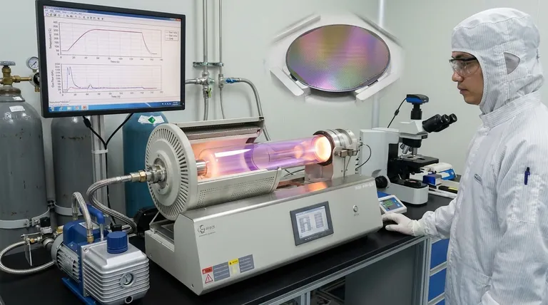
Visual Guide

Related Products
- Custom Made Versatile CVD Tube Furnace Chemical Vapor Deposition CVD Equipment Machine
- Split Chamber CVD Tube Furnace with Vacuum Station CVD Machine
- Multi Heating Zones CVD Tube Furnace Machine for Chemical Vapor Deposition Equipment
- Slide PECVD Tube Furnace with Liquid Gasifier PECVD Machine
- Inclined Rotary Plasma Enhanced Chemical Deposition PECVD Tube Furnace Machine
People Also Ask
- What is a CVD tube furnace and what is its primary function? Discover Precision Thin-Film Deposition
- What are the practical applications of gate media prepared by CVD tube furnaces? Unlock Advanced Electronics and More
- Why are CVD tube furnace sintering systems indispensable for 2D material research and production? Unlock Atomic-Scale Precision
- How does CVD tube furnace sintering enhance graphene growth? Achieve Superior Crystallinity and High Electron Mobility
- What customization options are available for CVD tube furnaces? Tailor Your System for Superior Material Synthesis


