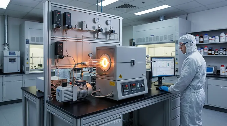
At its core, a Chemical Vapor Deposition (CVD) furnace is a highly specialized tool used in industries where the performance of a material is defined at the atomic level. Its primary applications are found in the semiconductor, aerospace, energy, and advanced materials sectors, where it is used to deposit ultra-pure, high-performance thin films onto various substrates.
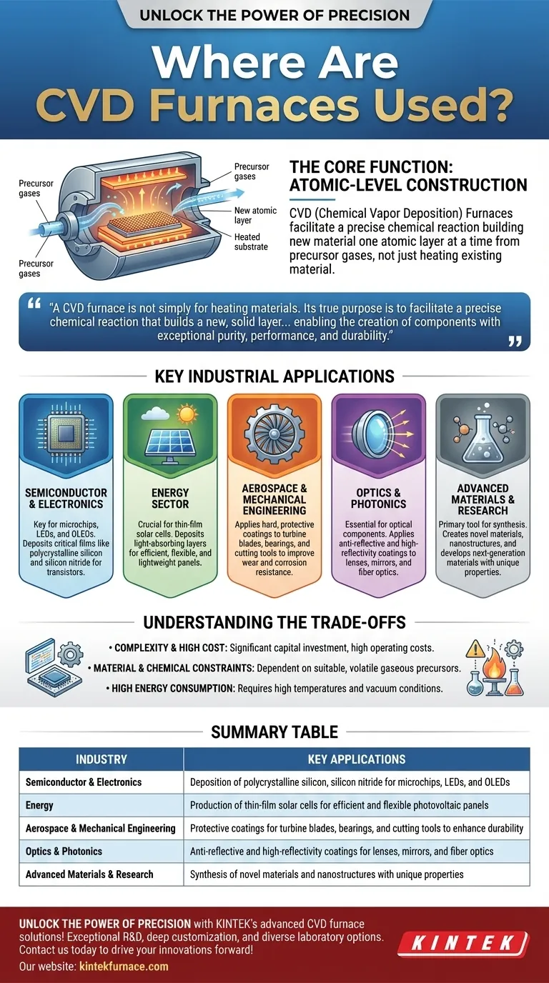
A CVD furnace is not simply for heating materials. Its true purpose is to facilitate a precise chemical reaction that "builds" a new, solid layer of material from a gas, enabling the creation of components with exceptional purity, performance, and durability.
The Core Function: Atomic-Level Construction
To understand where CVD furnaces are used, you must first understand what they do. Unlike a conventional furnace that just applies heat, a CVD furnace creates a highly controlled environment for a specific chemical process.
Moving Beyond Simple Heat Treatment
A standard furnace heats a solid to change its properties, such as hardening steel or firing ceramics. It modifies what is already there.
A CVD furnace, however, is a generative tool. It introduces new material to a substrate, building a thin film on its surface one layer of atoms at a time.
Building with Gaseous Precursors
The process involves introducing one or more volatile precursor gases into the furnace chamber. When these gases come into contact with the heated substrate, they react or decompose.
This chemical reaction causes a solid material to be deposited onto the substrate's surface, forming a thin, uniform film. The excess gaseous byproducts are then vented out of the chamber.
The Result: Ultra-Pure, High-Performance Films
This method allows for incredible control over a film's thickness, composition, and purity. The resulting coatings can provide properties—such as electrical conductivity, insulation, hardness, or corrosion resistance—that the underlying substrate lacks.
Key Industrial Applications
The ability to engineer materials at this level makes CVD technology indispensable across several high-tech industries.
The Semiconductor and Electronics Industry
This is the most significant user of CVD technology. Microchips are built by depositing alternating layers of conductive, insulating, and semiconducting materials.
CVD is used to deposit critical films like polycrystalline silicon and silicon nitride, which form the fundamental structures of transistors and other microelectronic components. It is also used in manufacturing LEDs and OLEDs for modern displays.
The Energy Sector
CVD is crucial for producing thin-film solar cells. The process deposits the light-absorbing semiconductor layers onto a substrate like glass or plastic.
This technique allows for the creation of efficient, flexible, and lightweight solar panels, which are a cornerstone of advancing photovoltaic technology.
Aerospace and Mechanical Engineering
In aerospace and manufacturing, components are often exposed to extreme temperatures, friction, and corrosive environments.
CVD is used to apply exceptionally hard and protective coatings to parts like turbine blades, bearings, and cutting tools. These coatings dramatically improve wear resistance, extend component life, and enhance performance.
Optics and Photonics
The performance of optical components like lenses, mirrors, and fiber optic cables depends on specialized surface coatings.
CVD is used to apply anti-reflective, high-reflectivity, or protective coatings that precisely control how light interacts with the surface, a critical function in everything from telescopes to telecommunications.
Advanced Materials and Research
In materials science and nanotechnology, CVD is a primary tool for synthesis. Researchers use it to create novel materials with unique properties, fabricate nanostructures, and develop the next generation of materials for a wide range of applications.
Understanding the Trade-offs
While powerful, CVD technology is not a universal solution. Its application comes with specific constraints and challenges.
Complexity and High Cost
CVD systems are complex machines that require precise control over temperature, pressure, and gas flow. They represent a significant capital investment and have high operating costs compared to simpler heat-treatment furnaces.
Material and Chemical Constraints
The CVD process is entirely dependent on the availability of suitable gaseous precursors. For some desired materials, a stable, volatile precursor chemical may not exist or may be prohibitively expensive or toxic, making deposition impractical.
High Energy Consumption
Achieving and maintaining the high temperatures (often over 1000°C) and vacuum conditions necessary for the chemical reactions requires a substantial amount of energy.
Making the Right Choice for Your Goal
Understanding the role of CVD is about recognizing its function as a high-precision manufacturing process, not just a heating device.
- If your primary focus is electronics or computing: CVD is the foundational technology for building the microchips that power the digital world.
- If your primary focus is manufacturing or aerospace: CVD is a key enabling technology for enhancing the durability and performance of critical components.
- If your primary focus is renewable energy: CVD is essential for producing the next generation of efficient and versatile thin-film solar cells.
- If your primary focus is materials science or research: CVD is a fundamental tool for synthesizing novel materials with precisely engineered properties.
Ultimately, the use of CVD furnaces signals a need to construct materials with a level of purity and structural control that is simply unattainable by other means.
Summary Table:
| Industry | Key Applications |
|---|---|
| Semiconductor & Electronics | Deposition of polycrystalline silicon, silicon nitride for microchips, LEDs, and OLEDs |
| Energy | Production of thin-film solar cells for efficient and flexible photovoltaic panels |
| Aerospace & Mechanical Engineering | Protective coatings for turbine blades, bearings, and cutting tools to enhance durability |
| Optics & Photonics | Anti-reflective and high-reflectivity coatings for lenses, mirrors, and fiber optics |
| Advanced Materials & Research | Synthesis of novel materials and nanostructures with unique properties |
Unlock the power of precision with KINTEK's advanced CVD furnace solutions! Leveraging exceptional R&D and in-house manufacturing, we provide diverse laboratories with high-temperature furnace options, including CVD/PECVD Systems, Muffle, Tube, Rotary, Vacuum & Atmosphere Furnaces. Our strong deep customization capability ensures we precisely meet your unique experimental requirements, delivering ultra-pure thin films and enhanced performance for industries like semiconductor, aerospace, and energy. Ready to elevate your materials engineering? Contact us today to discuss how our tailored solutions can drive your innovations forward!
Visual Guide
Related Products
- Custom Made Versatile CVD Tube Furnace Chemical Vapor Deposition CVD Equipment Machine
- Split Chamber CVD Tube Furnace with Vacuum Station CVD Machine
- Multi Heating Zones CVD Tube Furnace Machine for Chemical Vapor Deposition Equipment
- Slide PECVD Tube Furnace with Liquid Gasifier PECVD Machine
- Controlled Inert Nitrogen Hydrogen Atmosphere Furnace
People Also Ask
- How might AI and machine learning enhance CVD tube furnace processes? Boost Quality, Speed, and Safety
- What future trends are expected in the development of CVD tube furnaces? Discover Smarter, More Versatile Systems
- What is a CVD tube furnace and what is its primary function? Discover Precision Thin-Film Deposition
- What are the benefits of developing new precursor materials for CVD tube furnaces? Unlock Advanced Thin-Film Synthesis
- What are the key application fields of CVD tube furnaces? Unlock Precision in Thin-Film Synthesis


