Tin (Sn) doping fundamentally alters the thermoelectric behavior of bismuth micro-wires by re-engineering their electronic structure. At just 0.01–0.07 at% Sn, the Fermi level is driven deeper into the L‑valence band, effectively switching off light electron transport and flipping the thermoelectric voltage to a large positive value. In wires with optimized dimensions, this can push the thermo‑e.m.f. to 100–120 µV/K at 100 K and boost the one‑dimensional thermoelectric figure of merit by up to a factor of three. Realizing these gains reliably demands controlled vacuum or inert‑atmosphere thermal processing to prevent oxidation and to crystallize wires with uniform dopant distribution and high structural perfection.
By introducing tiny, carefully controlled amounts of Sn, you convert bismuth from a semimetal with mixed electron‑hole conduction into a system where holes dominate. The resulting shift in the Fermi level, amplified by quantum size effects in micro‑wires, yields a dramatic increase in thermoelectric performance—but only if the material is processed under conditions that eliminate oxidation and preserve crystalline quality.
The Physics: How Sn Redefines Bismuth’s Electronic Fermi Surface
Bismuth’s Native Semimetallic Band Structure
Pure bismuth is a semimetal with a small band overlap between the L‑point conduction band and the T‑point valence band.
This creates two carrier populations: light electrons at L and heavy holes at T, which together produce a near‑zero net thermo‑e.m.f. and limit the thermoelectric figure of merit.
Sn Acts as an Acceptor Dopant
Substituting a Bi atom with a Sn atom introduces an extra hole, because Sn has one fewer valence electron.
Even at concentrations as low as 0.01–0.07 at%, this acceptor doping shifts the Fermi level from the conduction‑band edge deep into the L‑valence band.
The primary reference confirms that this shift suppresses light electron carrier participation—the electron pocket is depopulated, and the conduction becomes overwhelmingly hole‑dominated.
Consequence: A Dramatic Swing in Thermoelectric Polarity
With electrons effectively removed from transport, the Seebeck coefficient turns from slightly negative or even positive to a strongly positive thermo‑e.m.f.
In the right wire geometry, the positive signal can rise to magnitudes of 100–120 µV/K at cryogenic temperatures, reflecting pure hole‑type conduction.
Quantum Size Effects: The Amplifier in Micro‑Wires
Confinement Enhances Thermoelectric Efficiency
When the wire diameter approaches the carrier de Broglie wavelength, transverse momentum becomes quantized.
This creates sharp features in the density of states that can dramatically increase the Seebeck coefficient and the dimensionless figure of merit.
The Combined Effect: Sn Doping + Dimensional Confinement
The reference demonstrates that in Bi‑0.02 at% Sn wires, quantum size effects cause the already‑large positive thermo‑e.m.f. to spike further.
The result is up to a 3‑fold increase in the thermoelectric figure of merit (Z₁DT) compared to thicker wires of the same composition—a gain that neither doping nor confinement alone could deliver.
Why Vacuum Thermal Processing Is Non‑Negotiable
Oxidation: The Silent Property Killer
Bismuth oxidizes rapidly at elevated temperatures.
A surface oxide layer introduces an uncontrolled parallel conduction path and destroys the precise carrier balance that doping was meant to set.
Recrystallization Annealing Under Controlled Atmosphere
To achieve the high structural perfection and uniform dopant concentration cited in the primary reference, the wires must undergo recrystallization annealing at high temperature.
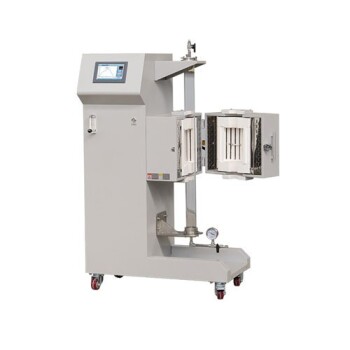
A high‑temperature vacuum tube furnace or an ultra‑pure inert‑atmosphere furnace is essential—it prevents oxidation, avoids contamination, and allows the dopant atoms to distribute homogeneously without evaporating.
Understanding the Trade‑offs and Pitfalls
- The doping window is extremely narrow. Exceeding ~0.07 at% Sn can cause phase segregation, severely reduce carrier mobility, and negate the thermoelectric gains.
- Ultra‑thin wires are susceptible to surface scattering. If the diameter is too small, diffuse surface scattering can lower electrical conductivity more than the quantum size boost compensates.
- Vacuum processing increases cost and complexity. For research‑grade performance it is unavoidable, but scaling up must balance the added investment against the magnitude of the ZT improvement.
- Temperature control is critical. Excessive annealing temperature or duration may coarsen grains and evaporate Sn, undoing the uniform doping profile.
Making the Right Choice for Your Thermoelectric Project
- If your primary focus is maximizing low‑temperature ZT: Target Sn concentrations near 0.02 at% and wire diameters where quantum size effects are active, then perform a precise vacuum recrystallization anneal to perfect the crystal and dopant distribution.
- If you aim for consistent, reproducible device performance: Invest in a high‑purity vacuum or inert‑gas furnace; the process control it provides is the only way to reliably suppress oxidation and lock in the Fermi‑level shift.
- If cost and scalability are early‑stage priorities: Start with a flowing‑inert‑atmosphere furnace to limit oxide formation during synthesis, but acknowledge that achieving the full 3‑fold ZT enhancement will likely require the superior environment of a vacuum system.
Mastering the interplay between Sn doping and controlled vacuum processing unlocks the full potential of bismuth micro‑wires as record‑setting thermoelectric elements at cryogenic temperatures.
Summary Table:
| Parameter / Feature | Influence of Sn Doping & Quantum Confinement | Role of Controlled Vacuum Thermal Processing |
|---|---|---|
| Electronic Structure | Shifts Fermi level into L-valence band, suppressing light electrons | Prevents surface oxidation and unwanted parallel conduction |
| Thermo-e.m.f. Output | Flips polarity to strongly positive (100–120 µV/K at 100 K) | Maintains exact dopant concentration and phase purity |
| Figure of Merit ($Z_1DT$) | Yields up to a 3-fold increase combined with size confinement | Allows high-temp recrystallization without Sn evaporation |
| Structural Perfection | Enhanced hole-dominated transport via quantum size effects | Ensures uniform dopant distribution and high crystal quality |
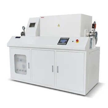
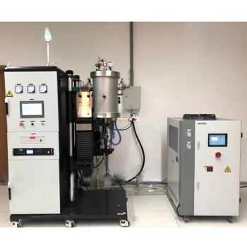
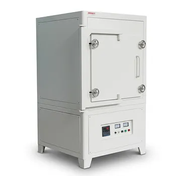
Ready to unlock record thermoelectric performance in your material synthesis? KINTEK specializes in advanced laboratory equipment and consumables, offering customizable high-temperature furnaces—including high-vacuum tube, inert atmosphere, muffle, and CVD systems—engineered to prevent oxidation and ensure precise thermal processing for micro-wire recrystallization. Enhance your research precision and material quality—contact us today to discuss your customized furnace requirements!
Related Products
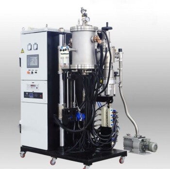
- Small Vacuum Heat Treat and Tungsten Wire Sintering Furnace
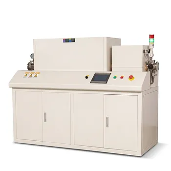
- Magnesium Extraction and Purification Condensing Tube Furnace
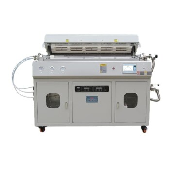
- Multi Heating Zones CVD Tube Furnace Machine for Chemical Vapor Deposition Equipment
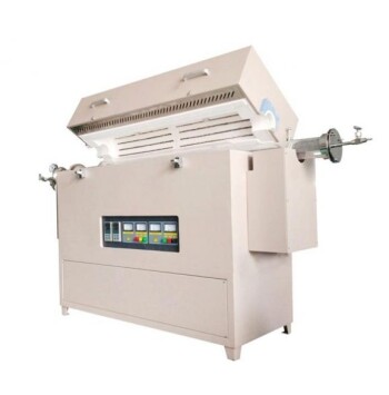
- Multi Zone Laboratory Quartz Tube Furnace Tubular Furnace
- Vertical Laboratory Quartz Tube Furnace Tubular Furnace
People Also Ask
- How does vacuum sintering improve dimensional tolerances? Achieve Uniform Shrinkage and Precision
- What are the key components of a vacuum sintering furnace? Essential Parts for Precision Material Processing
- What is the purpose of setting a mid-temperature dwell stage? Eliminate Defects in Vacuum Sintering
- What are the main structural components of a vacuum sintering furnace? Unlock Precision in High-Temperature Processing
- What are the main types of sintering furnaces? Find the Perfect Match for Your Materials