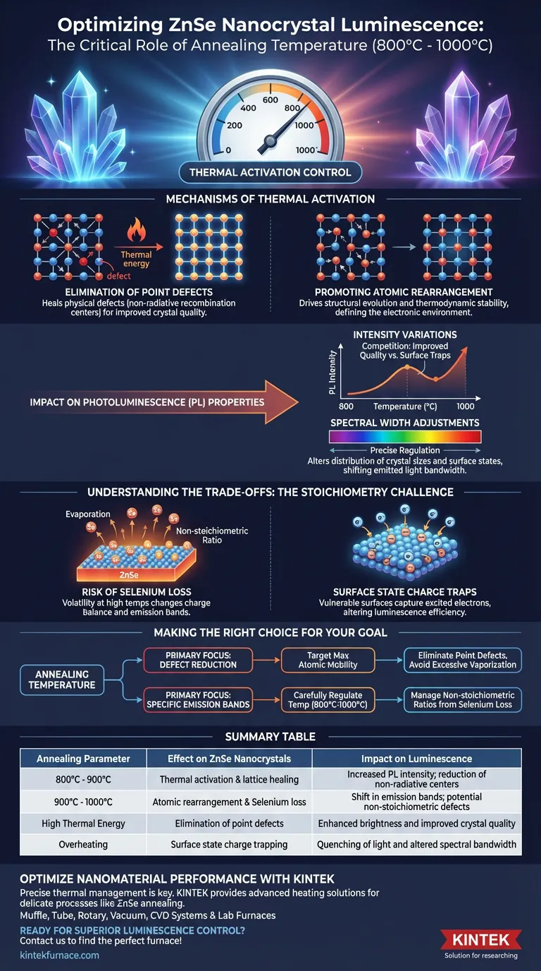
The temperature of the annealing process acts as a critical tuning mechanism for the optical properties of zinc selenide (ZnSe) nanocrystals. By adjusting thermal activation between 800°C and 1000°C, you directly manipulate photoluminescence (PL) intensity and spectral width through the elimination of point defects and the induction of atomic rearrangement.
The control of luminescence in ZnSe nanocrystals is a balancing act between structural repair and chemical stability. While high temperatures heal physical defects to improve crystal quality, they also induce Selenium loss, creating non-stoichiometric shifts that alter specific emission bands.
The Mechanisms of Thermal Activation
Elimination of Point Defects
The primary function of high-temperature annealing is thermal activation.
At elevated temperatures, the thermal energy supplied to the nanocrystals is sufficient to mobilize atoms within the lattice.
This mobility allows the material to "heal" itself, effectively removing point defects that often act as non-radiative recombination centers, which would otherwise quench luminescence.
Promoting Atomic Rearrangement
Beyond simple defect repair, annealing drives significant structural evolution.
The process promotes atomic rearrangement, allowing the crystal lattice to settle into a more thermodynamically stable state.
This structural relaxation is essential for defining the final electronic environment of the nanocrystal, which dictates how it interacts with light.
Impact on Photoluminescence (PL) Properties
Intensity Variations
As the annealing temperature increases from 800°C to 1000°C, the intensity of the photoluminescence changes efficiently.
This fluctuation is not linear; it reflects the competition between improved crystal quality (which boosts brightness) and surface trap formation (which can reduce it).
Spectral Width Adjustments
Temperature control allows for the precise regulation of the spectral width of the emission.
Changes in the annealing temperature alter the distribution of crystal sizes and surface states.
Consequently, the "color" or bandwidth of the emitted light shifts, allowing you to tune the material for specific optical applications.
Understanding the Trade-offs: The Stoichiometry Challenge
The Risk of Selenium Loss
A critical side effect of high-temperature annealing in ZnSe is the volatility of Selenium.
As temperatures approach 1000°C, the material is prone to losing Selenium atoms, leading to a non-stoichiometric chemical ratio.
This loss changes the charge balance within the crystal, directly impacting the emission bands and potentially introducing new, unwanted defect states.
Surface State Charge Traps
While internal defects may be healed, the surface of the nanocrystal remains vulnerable.
The annealing process modifies surface state charge trapping centers.
If not controlled, these traps can capture excited electrons before they emit light, altering the efficiency and character of the luminescence.
Making the Right Choice for Your Goal
To optimize the luminescence of ZnSe nanocrystals, you must select an annealing temperature that aligns with your specific optical requirements.
- If your primary focus is defect reduction: Target temperatures that maximize atomic mobility to eliminate point defects without inducing excessive vaporization.
- If your primary focus is specific emission bands: Carefully regulate the temperature between 800°C and 1000°C to manage the non-stoichiometric ratios caused by Selenium loss.
Precise thermal management is the difference between a high-performing optical component and a chemically unstable material.
Summary Table:
| Annealing Parameter | Effect on ZnSe Nanocrystals | Impact on Luminescence |
|---|---|---|
| 800°C - 900°C | Thermal activation & lattice healing | Increased PL intensity; reduction of non-radiative centers |
| 900°C - 1000°C | Atomic rearrangement & Selenium loss | Shift in emission bands; potential non-stoichiometric defects |
| High Thermal Energy | Elimination of point defects | Enhanced brightness and improved crystal quality |
| Overheating | Surface state charge trapping | Quenching of light and altered spectral bandwidth |
Optimize Your Nanomaterial Performance with KINTEK
Precise thermal management is the difference between high-performing optical components and chemical instability. KINTEK provides the advanced heating solutions required to master delicate processes like ZnSe annealing.
Backed by expert R&D and manufacturing, KINTEK offers Muffle, Tube, Rotary, Vacuum, and CVD systems, along with other lab high-temp furnaces—all fully customizable to meet your unique research or production needs.
Ready to achieve superior luminescence control? Contact us today to find the perfect furnace for your lab!
Visual Guide
References
- Aiman Akylbekovа, А. Usseinov. RAMAN ANALYSIS OF NANOCRYSTALS BASED ON ZINC SELENIDE. DOI: 10.52676/1729-7885-2023-4-77-84
This article is also based on technical information from Kintek Furnace Knowledge Base .
Related Products
- Controlled Inert Nitrogen Hydrogen Atmosphere Furnace
- Chairside Dental Porcelain Zirconia Sintering Furnace with Transformer for Ceramic Restorations
- Dental Porcelain Zirconia Sintering Ceramic Vacuum Press Furnace
- Spark Plasma Sintering SPS Furnace
- Vacuum Heat Treat Sintering Furnace Molybdenum Wire Vacuum Sintering Furnace
People Also Ask
- What are the characteristics and uses of hydrogen atmosphere in furnaces? Achieve Superior Surface Purity and Bonding
- What role do atmosphere furnaces play in the electronics sector? Essential for Semiconductor Fabrication
- How does a vacuum or controlled atmosphere furnace facilitate sessile-drop experiments? Optimize Alloy Wetting Analysis
- What environmental benefits do controlled atmosphere furnaces offer? Reduce Waste and Boost Efficiency
- How does a controlled atmosphere furnace contribute to energy efficiency? Lower Costs with Advanced Thermal Management