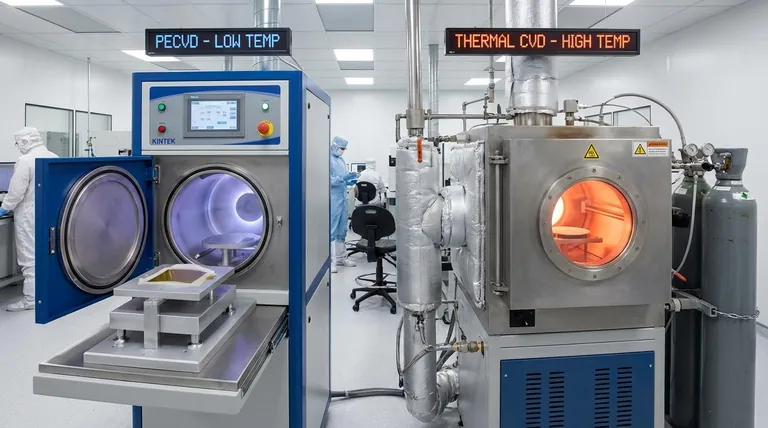
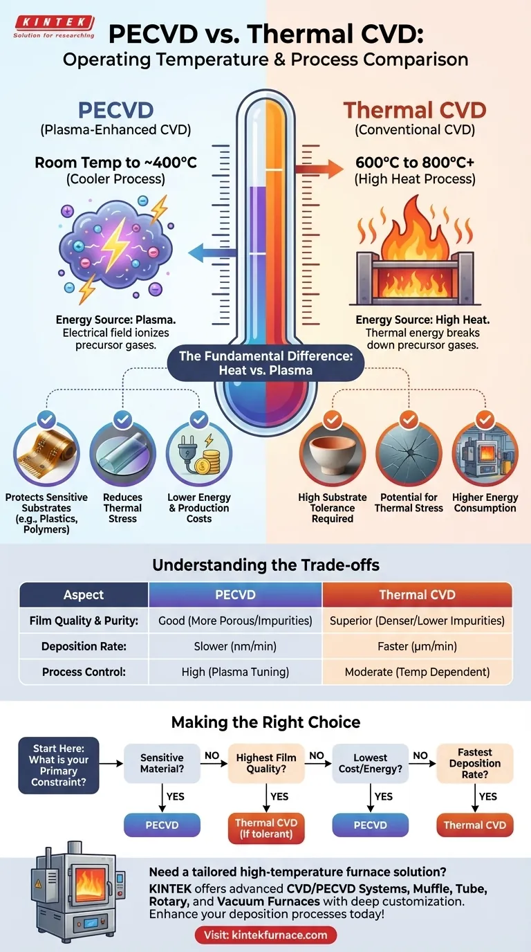
In short, Plasma-Enhanced Chemical Vapor Deposition (PECVD) operates at significantly lower temperatures than conventional thermal Chemical Vapor Deposition (CVD). PECVD processes typically run from room temperature up to around 400°C, whereas thermal CVD requires much higher temperatures, often between 600°C and 800°C, and sometimes even higher.
The core difference is the energy source. Thermal CVD relies exclusively on high heat to initiate chemical reactions, while PECVD uses an energy-rich plasma to achieve the same goal, allowing for deposition on temperature-sensitive materials that would be damaged by thermal processes.
The Fundamental Difference: Heat vs. Plasma
The operating temperature is not just a minor detail; it reflects the fundamental mechanism of each deposition technique. The choice between them is dictated by how energy is supplied to the precursor gases.
How Thermal CVD Works
Thermal CVD is conceptually straightforward. It uses high temperatures to provide the thermal energy needed to break down precursor gases and drive the chemical reactions that deposit a thin film onto a substrate.
This process typically requires substrate temperatures between 600°C and 800°C, and sometimes much higher, to achieve the necessary reaction kinetics. The heat is the sole catalyst for the deposition.
How PECVD Works
PECVD introduces a crucial alternative: plasma. Instead of relying on heat, an electrical field is used to ionize the precursor gases, creating a plasma filled with high-energy electrons, ions, and free radicals.
These energized particles collide with gas molecules, breaking chemical bonds and enabling deposition reactions to occur at much lower substrate temperatures. This allows PECVD to operate in a range from room temperature to about 350-400°C.
Why Lower Temperature Matters
The ability of PECVD to operate at lower temperatures is its primary advantage and opens up a range of applications that are impossible for thermal CVD.
Protecting Sensitive Substrates
The most significant benefit is compatibility with temperature-sensitive substrates. Materials like plastics, polymers, or devices with pre-existing metallic layers cannot withstand the extreme heat of thermal CVD. PECVD allows for coating these materials without causing melting, decomposition, or damage.
Reducing Thermal Stress
Even for substrates that can withstand high temperatures, the extreme heat of thermal CVD can induce significant thermal stress. This stress can cause film cracking, delamination, or warping, especially when depositing multiple layers with different thermal expansion coefficients. The gentler temperatures of PECVD minimize these risks.
Lowering Energy and Production Costs
Heating a reaction chamber to 800°C consumes a substantial amount of energy. By operating at lower temperatures, PECVD processes are inherently more energy-efficient, which can lead to significant reductions in production costs over time.
Understanding the Trade-offs
While lower temperature is a major advantage, it is not without compromises. The choice between PECVD and thermal CVD involves balancing temperature constraints against film quality and deposition speed.
Film Quality and Purity
Higher deposition temperatures generally produce higher-quality films. The heat used in thermal CVD helps create denser films with lower impurity levels (like hydrogen) and better structural integrity.
PECVD films, deposited at lower temperatures, can sometimes be more porous, contain more hydrogen, and be more susceptible to defects like pinholes. They may also have faster etch rates, indicating a less dense structure.
Deposition Rate
Thermal CVD often has a much higher deposition rate than PECVD. It can deposit films at tens of nanometers to several micrometers per minute.
In contrast, PECVD is typically a slower process, with deposition rates of a few to tens of nanometers per minute.
Process Control
The use of plasma in PECVD provides an additional level of control over the film's properties. By adjusting plasma power, frequency, and gas flow rates, operators can fine-tune characteristics like stress, density, and refractive index, independent of temperature.
Making the Right Choice for Your Goal
Your decision should be based on a clear understanding of your project's primary constraint.
- If your primary focus is depositing on a temperature-sensitive material: PECVD is the only viable choice.
- If your primary focus is achieving the highest possible film quality and purity: Thermal CVD is often superior, provided your substrate can tolerate the heat.
- If your primary focus is minimizing operational costs and energy usage: PECVD's lower temperature requirements make it the more economical option.
- If your primary focus is process speed for thick films: Thermal CVD generally offers a significant advantage in deposition rate.
Ultimately, selecting the right method requires balancing the need for low-temperature processing against the desired film quality and manufacturing efficiency.
Summary Table:
| Aspect | PECVD | Thermal CVD |
|---|---|---|
| Operating Temperature | Room temp to ~400°C | 600°C to 800°C or higher |
| Energy Source | Plasma | High heat |
| Key Advantage | Works with temperature-sensitive materials | Higher film quality and purity |
| Deposition Rate | Slower (nanometers per minute) | Faster (micrometers per minute) |
| Film Quality | May have more defects (e.g., pinholes) | Denser, lower impurity levels |
| Ideal Use Case | Substrates like plastics, polymers | High-temp tolerant substrates for superior films |
Need a high-temperature furnace solution tailored to your lab's unique needs? KINTEK leverages exceptional R&D and in-house manufacturing to provide advanced solutions like CVD/PECVD Systems, Muffle, Tube, Rotary, Vacuum & Atmosphere Furnaces. Our strong deep customization capability ensures precise fit for your experimental requirements, whether you're working with sensitive materials or demanding high-purity films. Contact us today to discuss how we can enhance your deposition processes and boost efficiency!
Visual Guide
Related Products
- Slide PECVD Tube Furnace with Liquid Gasifier PECVD Machine
- RF PECVD System Radio Frequency Plasma Enhanced Chemical Vapor Deposition
- Inclined Rotary Plasma Enhanced Chemical Deposition PECVD Tube Furnace Machine
- Inclined Rotary Plasma Enhanced Chemical Deposition PECVD Tube Furnace Machine
- Multi Heating Zones CVD Tube Furnace Machine for Chemical Vapor Deposition Equipment
People Also Ask
- What are the advantages of using a tube furnace CVD system for Cu(111)/graphene? Superior Scalability and Quality
- What are the disadvantages of tube furnace cracking when processing heavy raw materials? Avoid Costly Downtime and Inefficiency
- How does a hydrogen reduction environment in an industrial tube furnace facilitate gold-copper alloy microspheres?
- In which industries is the tube furnace commonly used? Essential for Materials Science, Energy, and More
- What are the typical conditions for plasma-enhanced CVD processes? Achieve Low-Temperature Thin Film Deposition


