Yes, absolutely. Chemical Vapor Deposition (CVD) is not an isolated technology but a foundational process that can be powerfully combined with other fabrication techniques. This integration allows for the creation of composite materials and complex devices with properties that a single method could never achieve, enhancing everything from material performance to manufacturing efficiency.
The core principle is synergy: by integrating CVD with technologies like Physical Vapor Deposition (PVD), Atomic Layer Deposition (ALD), or lithography, you can overcome the inherent limitations of each individual process to engineer materials and structures with precisely tailored, superior characteristics.
Why Integrate Technologies with CVD?
The drive to combine fabrication methods stems from the need to solve problems that a single technique cannot. Integration moves beyond simple deposition to true materials engineering.
Overcoming Standalone Limitations
CVD is renowned for producing highly conformal and pure films. However, it often requires high temperatures, which can damage sensitive substrates.
Other methods, like PVD, can operate at lower temperatures but struggle to coat complex, three-dimensional shapes uniformly. Combining them allows you to leverage the best attributes of each.
Achieving Synergistic Material Properties
A single material rarely has every desired property. You might need a surface that is both extremely hard and highly corrosion-resistant, or a film that is both conductive and optically transparent.
By depositing successive layers using different techniques (CVD for one layer, PVD for another), you can build a composite stack that embodies the desired combination of physical, chemical, and electrical properties.
Enabling Complex Device Fabrication
Modern microelectronics, sensors, and nanodevices are not simple films; they are intricate, patterned, multi-layered structures.
Fabricating these devices requires a sequence of steps. CVD is often used to deposit a uniform functional layer, which is then patterned using a technique like nanoimprint lithography to create the final device architecture.
Key Integration Examples and Applications
Hybrid systems are designed to perform multiple process steps, often within the same vacuum environment, to create higher-quality interfaces and improve throughput.
CVD + PVD (Physical Vapor Deposition)
This is a classic combination for advanced coatings. PVD, which includes methods like sputtering, excels at creating very dense, hard, and wear-resistant layers.
By adding a conformal CVD layer, you can ensure complete coverage and corrosion protection, even on complex parts. This hybrid approach is common for tooling, aerospace components, and biomedical implants where both hardness and perfect encapsulation are critical.
CVD + ALD (Atomic Layer Deposition)
This integration is all about achieving ultimate precision. ALD builds films one atomic layer at a time, offering unparalleled control over thickness and conformality. However, it is an extremely slow process.
A common strategy is to use ALD to deposit an ultra-thin, perfect "seed" or interface layer, and then switch to the much faster CVD process to deposit the bulk of the film. This gives you atomic-level precision where it matters most (at the interface) without sacrificing manufacturing time.
CVD + Lithography
This combination is the foundation of semiconductor and nanodevice fabrication. The process typically involves using CVD to deposit a uniform thin film (e.g., silicon dioxide, silicon nitride) across an entire wafer.
Next, a patterning technique like photolithography or nanoimprint lithography is used to define a specific circuit or device pattern. This is followed by an etching step to remove the unwanted material, leaving behind the desired structure.
Understanding the Trade-offs and Challenges
While powerful, integrating technologies is not without its difficulties. A clear understanding of the challenges is crucial for successful implementation.
Process Compatibility
Each technique operates under different conditions. A CVD process might use precursor gases that could poison a PVD sputtering target, or require temperatures that are incompatible with the hardware of the other system.
Ensuring that the vacuum, temperature, and chemical environments of the combined processes are compatible is a major engineering challenge.
System Complexity and Cost
A hybrid system is inherently more complex than a standalone tool. It requires sophisticated control software, more intricate hardware, and multiple power sources and gas delivery lines.
This increased complexity leads to a higher initial capital investment and can increase maintenance requirements.
Interface Control
The boundary between layers deposited by two different methods is a critical region. Any contamination or mismatch in crystal structure at this interface can compromise the adhesion and performance of the entire film stack.
Achieving a clean, abrupt, and structurally sound interface requires precise control over the transition from one process to the next, often by keeping the substrate in a shared vacuum environment.
Making the Right Choice for Your Goal
The decision to pursue a hybrid process depends entirely on your end goal.
- If your primary focus is enhanced mechanical performance: A CVD + PVD system is ideal for creating coatings that are simultaneously hard, dense, and perfectly conformal.
- If your primary focus is atomic-level precision: A CVD + ALD integration allows you to build films with perfect interfaces and nanometer-scale control without sacrificing overall deposition speed.
- If your primary focus is fabricating complex devices: Combining CVD for film deposition with lithography for patterning is the fundamental workflow for creating microelectronics and nanostructures.
Ultimately, integrating CVD with other technologies transforms it from a simple deposition tool into a key component of an advanced manufacturing ecosystem.
Summary Table:
| Integration Type | Key Benefits | Common Applications |
|---|---|---|
| CVD + PVD | Combines conformal coverage with dense, hard layers | Tooling, aerospace components, biomedical implants |
| CVD + ALD | Achieves atomic-level precision with faster deposition | High-precision films, interface engineering |
| CVD + Lithography | Enables complex patterning for device fabrication | Semiconductors, sensors, nanodevices |
Ready to elevate your lab's capabilities with custom high-temperature furnace solutions? At KINTEK, we leverage exceptional R&D and in-house manufacturing to provide advanced systems like Muffle, Tube, Rotary, Vacuum & Atmosphere Furnaces, and CVD/PECVD Systems. Our strong deep customization capability ensures we precisely meet your unique experimental needs, helping you achieve superior material performance and efficiency. Contact us today to discuss how we can support your integration goals!
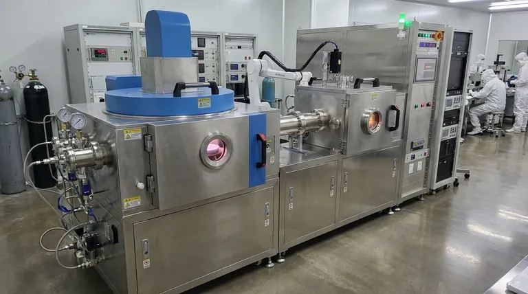
Visual Guide

Related Products
- Custom Made Versatile CVD Tube Furnace Chemical Vapor Deposition CVD Equipment Machine
- Split Chamber CVD Tube Furnace with Vacuum Station CVD Machine
- Multi Heating Zones CVD Tube Furnace Machine for Chemical Vapor Deposition Equipment
- Slide PECVD Tube Furnace with Liquid Gasifier PECVD Machine
- Controlled Inert Nitrogen Hydrogen Atmosphere Furnace
People Also Ask
- What are the key features of CVD tube furnaces for 2D material processing? Unlock Precision Synthesis for Superior Materials
- How might AI and machine learning enhance CVD tube furnace processes? Boost Quality, Speed, and Safety
- What customization options are available for CVD tube furnaces? Tailor Your System for Superior Material Synthesis
- Why are CVD tube furnace sintering systems indispensable for 2D material research and production? Unlock Atomic-Scale Precision
- What are the key application fields of CVD tube furnaces? Unlock Precision in Thin-Film Synthesis


