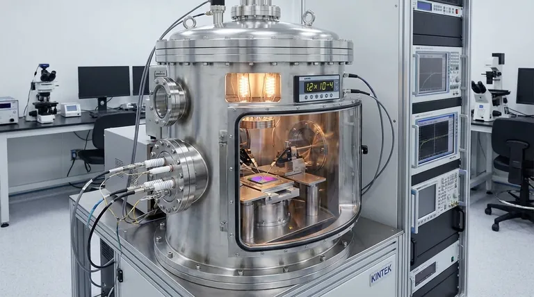
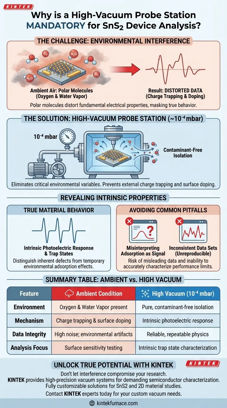
A high-vacuum probe station is a mandatory tool for the accurate electrical analysis of Tin Disulfide (SnS2) devices because it eliminates critical environmental variables. By operating at vacuum levels around 10^-4 mbar, the station removes polar molecules that otherwise distort the material's fundamental electrical properties.
By excluding oxygen and water vapor, high vacuum prevents external charge trapping and surface doping. This isolation enables researchers to distinguish the intrinsic photoelectric response of SnS2 from temporary environmental adsorption effects.
The Impact of Environmental Interference
The Culprits: Polar Molecules
The primary obstacles to accurate SnS2 analysis are environmental polar molecules.
Specifically, oxygen and water vapor present in ambient air are the main sources of interference.
Mechanisms of Distortion: Trapping and Doping
These molecules interact directly with the SnS2 surface.
This interaction leads to charge trapping and unintentional doping, which artificially alter the conductivity and responsiveness of the device.
Why High Vacuum is the Solution
Achieving the Correct Pressure
To effectively exclude these contaminants, the probe station must operate at specific vacuum levels.
The target pressure is approximately 10^-4 mbar, which is sufficient to strip the environment of interfering polar molecules.
Revealing Intrinsic Properties
The ultimate goal of using high vacuum is to observe the intrinsic photoelectric response of the material.
By removing the "noise" of environmental factors, researchers can clearly see the material's true behavior.
Isolating Trap States
Advanced analysis requires understanding the defects within the material itself.
Vacuum conditions allow you to distinguish between intrinsic trap states (inherent to the SnS2) and effects caused by external adsorption.
Common Pitfalls to Avoid
Misinterpreting Adsorption as Intrinsic Signal
If you analyze SnS2 in ambient air, you risk gathering misleading data.
A common error is attributing a specific electrical response to the material when it is actually caused by environmental adsorption.
Inconsistent Data Sets
Without vacuum control, fluctuations in humidity or oxygen levels can cause data inconsistency.
This makes it impossible to reproduce results or accurately characterize the device's performance limits.
Making the Right Choice for Your Goal
To ensure your research yields valid conclusions, align your testing environment with your specific objectives.
- If your primary focus is determining material physics: You must use high vacuum (10^-4 mbar) to measure intrinsic trap states without interference from oxygen or water.
- If your primary focus is characterizing surface sensitivity: You may compare vacuum measurements against ambient measurements to quantify the specific impact of environmental doping.
Using a high-vacuum environment is the only way to validate the true electrical identity of your SnS2 device.
Summary Table:
| Feature | Ambient Condition | High Vacuum (10^-4 mbar) |
|---|---|---|
| Environment | Oxygen & Water Vapor present | Pure, contaminant-free isolation |
| Mechanism | Charge trapping & surface doping | Intrinsic photoelectric response |
| Data Integrity | High noise; environmental artifacts | Reliable, repeatable physics |
| Analysis Focus | Surface sensitivity testing | Intrinsic trap state characterization |
Unlock the True Potential of Your Semiconductor Materials
Don't let environmental interference compromise your research. KINTEK provides high-precision lab solutions, including advanced vacuum systems tailored for the most demanding semiconductor characterization. Backed by expert R&D and manufacturing, we offer Muffle, Tube, Rotary, Vacuum, and CVD systems, all fully customizable to meet the unique needs of your SnS2 and 2D material studies.
Ready to achieve high-vacuum precision in your lab?
Contact KINTEK experts today to discuss your custom furnace or vacuum needs.
Visual Guide
References
- S. De Stefano, Antonio Di Bartolomeo. Neuromorphic Photoresponse in Ultrathin SnS<sub>2</sub>-Based Field Effect Transistor. DOI: 10.1021/acsami.5c11651
This article is also based on technical information from Kintek Furnace Knowledge Base .
Related Products
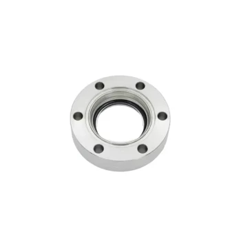
- Ultra High Vacuum CF Observation Window Flange with High Borosilicate Glass Sight Glass
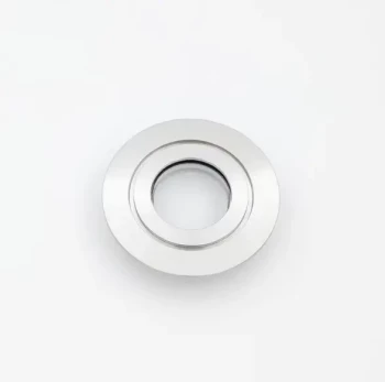
- Ultra High Vacuum Observation Window Stainless Steel Flange Sapphire Glass Sight Glass for KF
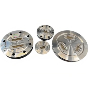
- Ultra-High Vacuum Flange Aviation Plug Glass Sintered Airtight Circular Connector for KF ISO CF
- High Performance Vacuum Bellows for Efficient Connection and Stable Vacuum in Systems
- 304 316 Stainless Steel High Vacuum Ball Stop Valve for Vacuum Systems
People Also Ask
- How does the pressure environment affect the metallic thermal reduction for titanium? Master Precision Control
- What are the structural functions of the dual-chamber quartz glass container? Optimize Magnesium Alloy Vapor Analysis
- What role does a closed pressure vessel play during the carbonation of gamma-C2S? Unlock Rapid Mineralization
- Why is an Ultra-High Vacuum (UHV) System Required for In2Se3? Achieving Atomic-Level Ferroelectric Clarity
- What is the purpose of utilizing a glassy carbon crucible and HCl gas treatment? Ensure Pure Molten Salt Systems