In short, Chemical Vapor Deposition (CVD) is an exceptionally versatile process capable of depositing a vast range of materials. These include pure elements like metals and silicon, complex compounds like ceramics (oxides, nitrides, carbides), and advanced nanostructures such as synthetic diamond, graphene, and carbon nanotubes. This flexibility makes it a cornerstone technology in fields from microelectronics to materials science.
CVD's power lies in its ability to synthesize materials directly on a surface from chemical precursors, offering immense flexibility. However, its primary limitation is the high process temperature required for many reactions, which dictates which substrates and applications are practical.
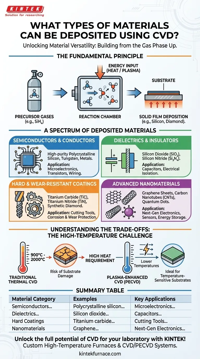
The Fundamental Principle: Building Materials from Gas
To understand what CVD can create, you must first understand how it works. It's a process of building a solid film from the bottom up, using chemical reactions rather than melting and spraying a source material.
The Role of Precursor Gases
The process begins by introducing one or more volatile precursor gases into a reaction chamber. These gases contain the atoms of the desired final material. For example, to deposit silicon, a precursor like silane (SiH₄) might be used.
Triggering the Chemical Reaction
Energy, typically in the form of very high heat, is applied to the chamber. This energy breaks down the precursor gases into reactive species.
Deposition on the Substrate
These reactive chemical species then deposit onto a heated object (the substrate) placed in the chamber. A chemical reaction occurs on the substrate's surface, forming a stable, solid thin film of the desired material.
A Spectrum of Deposited Materials
The chemical nature of CVD allows for the synthesis of an incredibly diverse material library, categorized by their properties and applications.
Semiconductors and Conductors
CVD is fundamental to the microelectronics industry. It is used to deposit high-purity polycrystalline silicon, which forms the basis of transistors, as well as conductive films like tungsten and other metals used for wiring in integrated circuits.
Dielectrics and Insulators
The process is also used to create electrically insulating layers. Materials like silicon dioxide (SiO₂) and silicon nitride (Si₃N₄) are deposited as dielectric layers in capacitors and to isolate conductive components from one another.
Hard and Wear-Resistant Coatings
CVD excels at creating exceptionally hard, durable coatings for mechanical parts and cutting tools. These include titanium carbide (TiC), titanium nitride (TiN), and famously, thin films of synthetic diamond, which protect surfaces from wear, corrosion, and oxidation.
Advanced Nanomaterials
Modern applications of CVD push the boundaries of materials science. It is a key method for growing advanced materials like graphene sheets, forests of carbon nanotubes (CNTs), and quantum dots, which have applications in next-generation electronics, sensors, and energy storage.
Understanding the Trade-offs: The High-Temperature Challenge
While powerful, CVD is not without significant constraints. The primary trade-off is the process temperature.
The High Heat Requirement
Traditional thermal CVD often operates at extremely high temperatures, typically between 900°C and 2000°C. This heat is necessary to provide the activation energy for the chemical reactions to occur.
Risk of Substrate Damage
These high temperatures can damage the underlying workpiece. It can cause deformation, unwanted structural changes, or a weakened bond between the coating and the substrate, limiting the types of materials that can be coated.
The Low-Temperature Solution: PECVD
To overcome this limitation, variants like Plasma-Enhanced CVD (PECVD) were developed. PECVD uses an electric field to create a plasma, which energizes the precursor gases at much lower temperatures. This enables the deposition of high-quality films on temperature-sensitive substrates like plastics or certain metal alloys.
Making the Right Choice for Your Goal
The material you can deposit is directly linked to the specific CVD process you choose and the limitations of your substrate.
- If your primary focus is ultimate purity and crystallinity: Traditional high-temperature CVD is the standard for materials like semiconductor-grade silicon or synthetic diamond, assuming your substrate can tolerate the heat.
- If your primary focus is coating temperature-sensitive materials: You must use a lower-temperature variant like Plasma-Enhanced CVD (PECVD) to avoid damaging the underlying part while depositing films like silicon nitride.
- If your primary focus is surface protection and hardness: CVD's ability to deposit extremely hard ceramic coatings like carbides and nitrides makes it ideal for enhancing the durability of tools and components that can withstand high temperatures.
Ultimately, mastering CVD means matching the right chemical precursors and process conditions to your specific material and substrate goals.
Summary Table:
| Material Category | Examples | Key Applications |
|---|---|---|
| Semiconductors and Conductors | Polycrystalline silicon, Tungsten | Microelectronics, Transistors, Wiring |
| Dielectrics and Insulators | Silicon dioxide (SiO₂), Silicon nitride (Si₃N₄) | Capacitors, Electrical Isolation |
| Hard and Wear-Resistant Coatings | Titanium carbide (TiC), Titanium nitride (TiN), Synthetic diamond | Cutting Tools, Corrosion Protection |
| Advanced Nanomaterials | Graphene, Carbon nanotubes (CNTs), Quantum dots | Next-Gen Electronics, Sensors, Energy Storage |
Unlock the full potential of CVD for your laboratory with KINTEK! Leveraging exceptional R&D and in-house manufacturing, we provide advanced high-temperature furnace solutions, including Muffle, Tube, Rotary Furnaces, Vacuum & Atmosphere Furnaces, and CVD/PECVD Systems. Our strong deep customization capability ensures we precisely meet your unique experimental requirements, whether you're working with semiconductors, nanomaterials, or wear-resistant coatings. Contact us today to discuss how our tailored solutions can enhance your research and development processes!
Visual Guide
Related Products
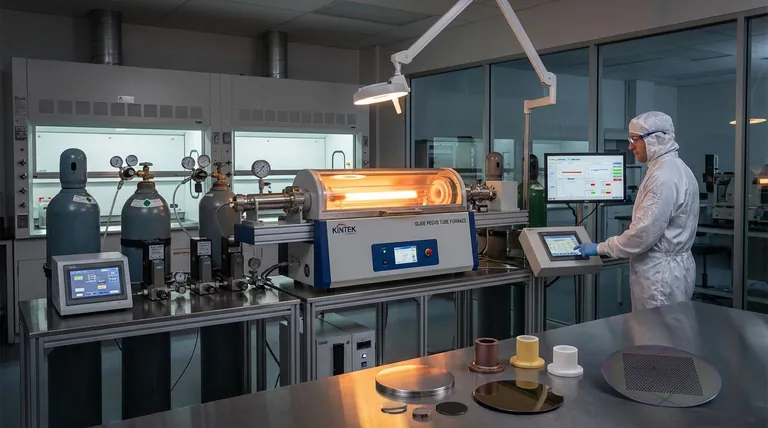
- Custom Made Versatile CVD Tube Furnace Chemical Vapor Deposition CVD Equipment Machine
- MPCVD Machine System Reactor Bell-jar Resonator for Lab and Diamond Growth
- Multi Heating Zones CVD Tube Furnace Machine for Chemical Vapor Deposition Equipment
- 915MHz MPCVD Diamond Machine Microwave Plasma Chemical Vapor Deposition System Reactor
- Slide PECVD Tube Furnace with Liquid Gasifier PECVD Machine
People Also Ask
- Why are CVD tube furnace sintering systems indispensable for 2D material research and production? Unlock Atomic-Scale Precision
- How does CVD tube furnace sintering enhance graphene growth? Achieve Superior Crystallinity and High Electron Mobility
- What temperature range do standard CVD tube furnaces operate at? Unlock Precision for Your Material Deposition
- What customization options are available for CVD tube furnaces? Tailor Your System for Superior Material Synthesis
- What is a CVD tube furnace and what is its primary function? Discover Precision Thin-Film Deposition


