Start with a narrow, almost "pointillist" view of the atomic interface, then zoom out to show how those microscopic mismatches create macroscopic, performance-killing defects—and how the furnace itself becomes the solution.
A 20% lattice mismatch and an 8–20% thermal expansion coefficient (CTE) mismatch between 3C-SiC and common substrates (Si, hexagonal SiC) directly nucleate stacking faults, double positioning boundaries, and electrically active inversion domain boundaries. Poor thermal ramp control then transforms those nucleation events into extended transition zones of mixed polytypes like 15R-SiC and 6H-SiC. The central mitigation strategy lies in advanced high-temperature CVD furnaces that enforce multi-zone uniformity, programmable multi-stage heating ramps, and precise axial thermal gradients (ideally below 5 K/mm)—turning the furnace from a simple heat source into a defect-suppression tool.
The deep challenge of 3C-SiC heteroepitaxy is not simply avoiding a single defect; it is managing a cascade of mismatched forces. Furnace design mitigates this by decoupling the thermal expansion response from the lattice accommodation, using ultra-controlled ramp rates and graded buffer layers to absorb strain elastically while keeping the axial temperature gradient low enough to favor the cubic polytype and suppress stacking fault proliferation.
Understanding the Root Causes of 3C-SiC Crystal Defects
Heteroepitaxial growth on silicon or hexagonal SiC seeds a host of structural imperfections. They originate from two fundamental mismatches that operate at different stress regimes.
The Lattice Mismatch: A Geometric Battleground
A lattice mismatch of up to 20% forces the growing 3C-SiC film to either stretch or compress violently at the interface. This creates an extremely high density of dislocations.
The energy is partially relieved by the formation of double positioning boundaries (DPBs) . These are twin-like boundaries where the stacking sequence of the cubic lattice is rotated, leading to electrically disruptive domains even if chemical purity is perfect.
Inversion domain boundaries (IDBs) emerge from homo-elemental wrong bonds—Si-Si and C-C—at the heterointerface. Unlike a simple structural defect, these are electrically active, pinning the Fermi level and degrading device performance.
The Thermal Expansion Mismatch: A Post-Growth Catastrophe
An 8% to 20% CTE mismatch means that as the film cools from the deposition temperature (>1500 °C), the substrate and epilayer contract at drastically different rates. The resulting tensile or compressive stress causes macroscopic wafer bowing, cracking, and delamination.
This stress can relax by generating additional stacking faults on {111} planes, many of which intersect the surface as linear defects. The correlation is direct: higher thermal gradients and faster cooling greatly multiply these faults.
The Critical Impact of Thermal Gradients on Polytype Purity
Defects are not only nucleated by mismatch; they are amplified by poor thermal control. The shape and symmetry of the thermal field during growth dictates polytype stability.
Axial Gradients and Stacking Fault Density
Vertical (axial) thermal gradients in the range of 5 to 8 K/mm significantly influence stacking fault density. Research shows that minimizing this gradient strongly favors the growth of pure 3C-SiC by suppressing the atomic plane mis-stacking that leads to other polytypes.
A steep gradient induces non-uniform gas-phase supersaturation near the surface and can trigger the insertion of hexagonal layers, forming complex twin structures and faulted domains that degrade optical and electronic quality.
The Danger of Uncontrolled Ramp-Up: Transitional Polytypes
Before steady-state growth, a poorly controlled temperature ramp-up creates a narrow window of intermediate temperatures where competing polytypes become thermodynamically accessible. This leads to a non-abrupt interface with transitional polytypic phases (15R-SiC and 6H-SiC) .
Once these polytype transients form, they propagate as extended defects into the overlying film, creating a chemically disorganised buffer that no amount of post-process annealing can remove. The primary reference is unequivocal: poor ramp-up thermal control is a direct root cause of this interlayering.
How High-Temperature CVD Furnace Features Mitigate These Challenges
The furnace becomes the first line of defense. Its architecture is engineered to directly counteract the mechanical and kinetic origins of defects.
Multi-Zone Heating Elements for Gradient Engineering
Multi-zone heating allows the operator to establish a precise, programmable axial thermal profile. This directly addresses the gradient dependency: you can target a thermal gradient significantly lower than 5 K/mm to minimise stacking faults.
Zone uniformity prevents lateral temperature variations across the substrate, ensuring that all areas experience the same strain state simultaneously. This is critical for keeping wafer bow under control during both ramp-up and cool-down, as localized cold spots act as stress concentrators.
Programmable Multi-Stage Thermal Ramps
Programmable multi-stage heating controllers are not a convenience; they are a defect-prevention prerequisite. They allow operators to insert holding steps at intermediate temperatures, enabling the growth of a buffer layer that accommodates lattice strain gradually before the main epitaxial layer is deposited.
Meticulous control of the ramp-up rate directly prevents the uncontrolled polytypic transitions described in the primary reference. Instead of passing through a chaotic thermal zone, the system dwells at a stable temperature, suppressing the nucleation of 15R-SiC or 6H-SiC seeds and forcing an abrupt 3C-SiC interface.
Atmosphere Control and Vacuum Integrity
A leak-tight vacuum flange assembly combined with integrated gas distribution manifolds prevents source-gas contamination. Oxygen or nitrogen back-streaming at >1500°C would form precipitates that act as potent heterogeneous nucleation sites for stacking faults.
Precursor delivery uniformity, enabled by these gas manifolds, maintains a stable carbon-to-silicon ratio at the growth surface. Fluctuations locally shift stoichiometry and can induce C-C or Si-Si wrong bonds, increasing the IDB density. A controlled atmosphere makes the surface chemistry as uniform as the thermal field.
Understanding the Trade-offs and Limitations
Even with an ideal furnace, physical constraints force a balance between throughput and perfection.
Growth rate vs. defect density. Lower growth rates typically yield higher crystalline quality because the adatoms have more time to find correct lattice sites, reducing DPB formation. However, this extends process time and increases material cost, requiring a careful economic trade-off.
Buffer layer thickness vs. final stress state. A thick, graded buffer layer compliantly absorbs more lattice mismatch at the interface, reducing dislocation density. Yet the same thermal expansion mismatch still applies; a complex stack of buffers can build up internal stress during cooling that ultimately bows the wafer more than a direct epitaxial layer. Furnace cool-down rates must be tailored to the specific buffer stack design.
Minimum gradient limits. While a lower gradient reduces stacking faults, an extremely flat gradient can slow precursor transport and degrade film thickness uniformity. The target gradient (often around 3–5 K/mm) is inherently a compromise between defect suppression and deposition rate control.
Making the Right Choice for Your Process Goal
Furnace feature selection will depend on which defect mechanism is the primary limiter for your device or application.
- If your primary focus is eliminating polytype intermixing: Invest in a system with high-precision programmable ramp controllers and implement a deliberate buffer layer growth step at a stable intermediate temperature to lock in the cubic phase before ramping to full growth temperature.
- If your primary focus is minimizing stacking fault density: Specify a furnace with a strong multi-zone vertical heating array capable of maintaining an axial thermal gradient reliably below 5 K/mm, and verify uniformity with high-resolution pyrometry across the load zone.
- If your primary focus is reducing macroscopic wafer bow: Ensure the furnace provides exceptional lateral zone uniformity and programmable, slow cool-down ramps that keep the thermal expansion stress below the critical resolved shear stress for glide on the basal plane.
The furnace you select is not merely a high-temperature enclosure but the precise thermal instrument that defines which defect physics will dominate your 3C-SiC film.
Summary Table:
| Defect / Challenge | Primary Root Cause | High-Temp Furnace Mitigation Feature |
|---|---|---|
| Stacking Faults & Polytype Intermixing (15R/6H-SiC) | Steep axial thermal gradients (>5 K/mm) & uncontrolled ramp-up | Multi-Zone Heating maintaining axial gradients <5 K/mm & programmable thermal ramps |
| Double Positioning & Inversion Domain Boundaries (IDBs) | ~20% lattice mismatch & interface wrong-bond formation | Multi-Stage Controllers enabling intermediate temperature steps for graded buffer layer growth |
| Wafer Bowing, Cracking & Delamination | 8–20% CTE mismatch during post-growth cooling | Lateral Zone Uniformity & programmable slow cool-down ramps to minimize thermal stress |
| Heterogeneous Stacking Fault Nucleation | Source-gas contamination (O2/N2) at >1500 °C | Leak-Tight Vacuum Assemblies & integrated gas distribution manifolds for precise C/Si control |
Maximize Your 3C-SiC Yield with Precision Furnace Engineering
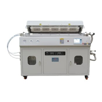
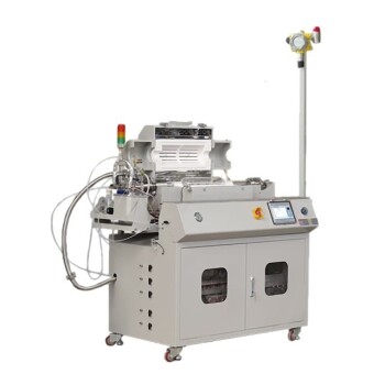
Eliminate polytype intermixing, wafer bow, and lattice defects in your heteroepitaxial processes. KINTEK specializes in advanced laboratory equipment and high-temperature furnace solutions—including state-of-the-art CVD, atmosphere, tube, and vacuum furnaces engineered with precise multi-zone temperature control and fully programmable thermal ramps.
Whether you require specialized standard equipment or custom-engineered furnace configurations tailored to your crystal growth parameters, KINTEK provides the reliability and precision your research demands.
👉 Contact KINTEK today to consult with our technical experts and discover how our tailored furnace solutions can optimize your process performance.
Related Products
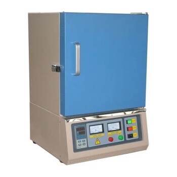
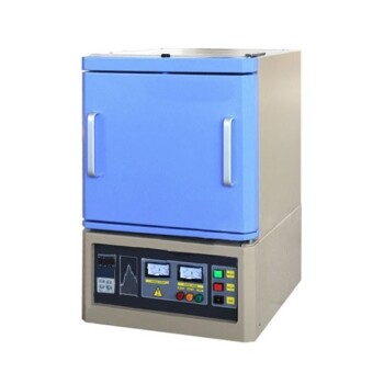
- 1400℃ Muffle Oven Furnace for Laboratory
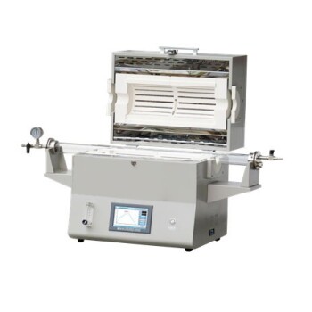
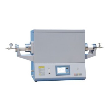
- 1400℃ High Temperature Laboratory Tube Furnace with Alumina Tube
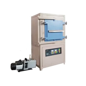
- 1700℃ Controlled Inert Nitrogen Atmosphere Furnace
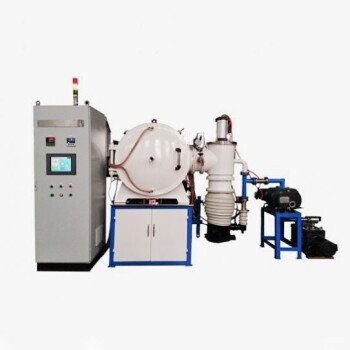
- 2200 ℃ Graphite Vacuum Heat Treat Furnace
- 1800℃ High Temperature Muffle Oven Furnace for Laboratory
People Also Ask
- What is the primary function of a high-temperature laboratory muffle furnace in chemical synthesis? Achieve Precision.
- How does a high-temperature laboratory muffle furnace affect material properties? Transform Anodic Oxide Films Fast
- How is a laboratory high-temperature muffle furnace utilized in g-C3N4 synthesis? Optimize Your Thermal Polycondensation
- What is the purpose of using a laboratory high-temperature muffle furnace for drying Fe-Ni-Co catalysts? Boost Purity
- What role does a laboratory high-temperature muffle furnace play in the treatment of highly contaminated waste glass?