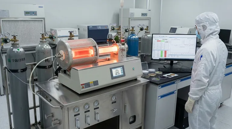
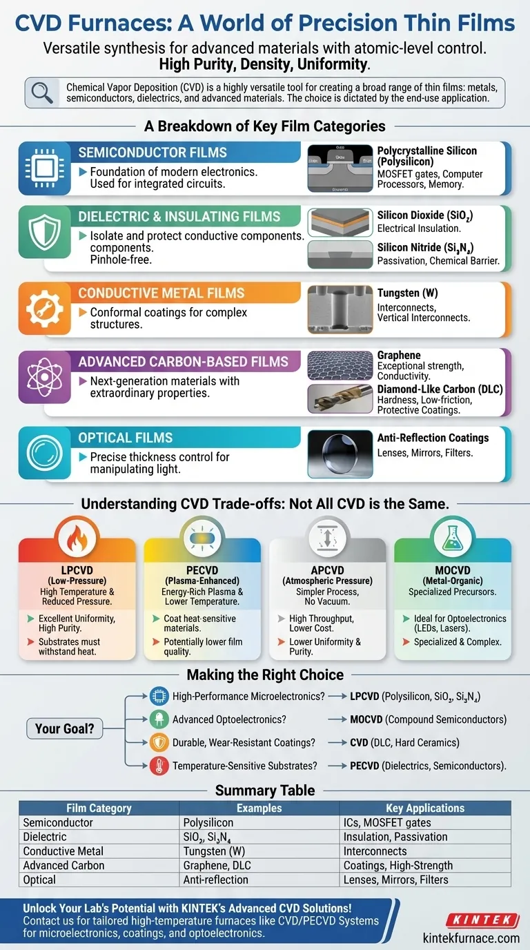
At its core, a Chemical Vapor Deposition (CVD) furnace is a highly versatile tool capable of synthesizing an exceptionally broad range of thin films with atomic-level precision. These films can be broadly categorized into metals, semiconductors, and dielectrics (like oxides, nitrides, and carbides), as well as advanced materials such as graphene and diamond-like carbon. The specific film choice is dictated entirely by the end-use application, from building microchips to creating durable protective coatings.
The true value of CVD is not just the variety of films it can create, but its ability to produce them with exceptional purity, density, and uniformity. This precision is what makes CVD indispensable for manufacturing high-performance electronic, optical, and mechanical components where material quality directly dictates function.
A Breakdown of Key Film Categories
CVD's versatility stems from its fundamental process: introducing reactive gases (precursors) into a chamber where they react and deposit a solid film onto a substrate. By carefully selecting these precursors and controlling conditions like temperature and pressure, we can engineer films with specific chemical compositions and properties.
Semiconductor Films
These materials are the foundation of all modern electronics. CVD is the dominant method for depositing the ultra-pure semiconductor layers required for integrated circuits.
A primary example is polycrystalline silicon (polysilicon), which is used to create the gate electrodes in Metal-Oxide-Semiconductor Field-Effect Transistors (MOSFETs), the building blocks of every computer processor and memory chip.
Dielectric and Insulating Films
Dielectric films do not conduct electricity and are critical for isolating and protecting conductive components in microdevices. CVD excels at creating dense, pinhole-free insulating layers.
Common examples include Silicon Dioxide (SiO₂) for electrical insulation and Silicon Nitride (Si₃N₄), which serves as a robust passivation layer, chemical barrier, and dielectric. Hard ceramic films like carbides can also be deposited for wear resistance.
Conductive Metal Films
While other methods exist for metal deposition, CVD can be used to create highly conformal metal layers that evenly coat complex, three-dimensional microstructures.
Tungsten (W) is a common example, used to fill microscopic vias and create vertical interconnects within a chip. Other metals can also be deposited depending on the required conductivity and chemical stability.
Advanced Carbon-Based Films
CVD is at the forefront of producing next-generation materials with extraordinary properties.
Two prominent examples are graphene, a single atomic layer of carbon with exceptional strength and conductivity, and Diamond-Like Carbon (DLC), an amorphous film that is extremely hard and low-friction, making it an ideal protective coating for tools, medical implants, and engine parts.
Optical Films
The precise thickness control offered by CVD is ideal for producing optical films. These are used to create coatings that manipulate light.
Applications include anti-reflection coatings on lenses, high-reflectivity mirrors, and specialized filters, where film thickness must be controlled down to a fraction of a wavelength of light.
Understanding the Trade-offs: Not All CVD is the Same
The term "CVD" describes a family of techniques. The specific process chosen involves critical trade-offs between deposition temperature, film quality, and cost. The type of furnace and process directly influences the films you can create.
Temperature vs. Quality (LPCVD vs. PECVD)
Low-Pressure CVD (LPCVD) operates at high temperatures and reduced pressure. This produces extremely uniform and high-purity films but is unsuitable for substrates that cannot withstand the heat.
Plasma-Enhanced CVD (PECVD) uses an energy-rich plasma to facilitate the chemical reaction. This allows deposition to occur at much lower temperatures, making it ideal for coating heat-sensitive materials, though film quality can sometimes be lower than that of high-temperature methods.
Pressure and Simplicity (APCVD)
Atmospheric Pressure CVD (APCVD) is a simpler, higher-throughput process that does not require expensive vacuum systems. However, the resulting film uniformity and purity are generally lower than what can be achieved with low-pressure systems.
Precursor Specificity (MOCVD)
Metal-Organic CVD (MOCVD) is a specialized variant that uses metal-organic compounds as precursors. It is the industry standard for manufacturing high-performance optoelectronics, such as creating the complex, multi-layered compound semiconductor films required for LEDs and laser diodes.
Making the Right Choice for Your Application
Your choice of film and CVD method must be driven by your final goal. There is no single "best" option, only the most appropriate one for the task.
- If your primary focus is high-performance microelectronics: You will likely require LPCVD to deposit ultra-pure polysilicon and dielectric films like SiO₂ and Si₃N₄ for transistor gates and insulation.
- If your primary focus is advanced optoelectronics (LEDs): MOCVD is the essential technique for growing the high-quality compound semiconductor layers needed to generate light efficiently.
- If your primary focus is durable, wear-resistant coatings: CVD deposition of Diamond-Like Carbon (DLC) or hard ceramics provides superior protection for mechanical parts and cutting tools.
- If your primary focus is depositing on temperature-sensitive substrates: PECVD is the clear choice, as it allows you to create quality dielectric or semiconductor films without damaging the underlying material.
Understanding these distinct capabilities allows you to leverage CVD not just as a deposition tool, but as a precise instrument for engineering materials from the atoms up.
Summary Table:
| Film Category | Examples | Key Applications |
|---|---|---|
| Semiconductor Films | Polycrystalline silicon (polysilicon) | Integrated circuits, MOSFET gates |
| Dielectric and Insulating Films | Silicon dioxide (SiO₂), Silicon nitride (Si₃N₄) | Electrical insulation, passivation layers |
| Conductive Metal Films | Tungsten (W) | Interconnects in microchips |
| Advanced Carbon-Based Films | Graphene, Diamond-like carbon (DLC) | Protective coatings, high-strength materials |
| Optical Films | Anti-reflection coatings | Lenses, mirrors, filters |
Unlock the full potential of your lab with KINTEK's advanced CVD furnace solutions! Leveraging exceptional R&D and in-house manufacturing, we provide diverse laboratories with high-temperature furnace options like CVD/PECVD Systems, tailored to meet your unique experimental needs. Whether you're developing microelectronics, durable coatings, or optoelectronics, our deep customization ensures precise film deposition for superior results. Contact us today to discuss how we can enhance your research and production efficiency!
Visual Guide
Related Products
- Custom Made Versatile CVD Tube Furnace Chemical Vapor Deposition CVD Equipment Machine
- Split Chamber CVD Tube Furnace with Vacuum Station CVD Machine
- Multi Heating Zones CVD Tube Furnace Machine for Chemical Vapor Deposition Equipment
- Slide PECVD Tube Furnace with Liquid Gasifier PECVD Machine
- Inclined Rotary Plasma Enhanced Chemical Deposition PECVD Tube Furnace Machine
People Also Ask
- What are the benefits of developing new precursor materials for CVD tube furnaces? Unlock Advanced Thin-Film Synthesis
- What is the working principle of a CVD tube furnace? Achieve Precise Thin Film Deposition for Your Lab
- What is a CVD tube furnace and what is its primary function? Discover Precision Thin-Film Deposition
- What are the key application fields of CVD tube furnaces? Unlock Precision in Thin-Film Synthesis
- What temperature range do standard CVD tube furnaces operate at? Unlock Precision for Your Material Deposition


