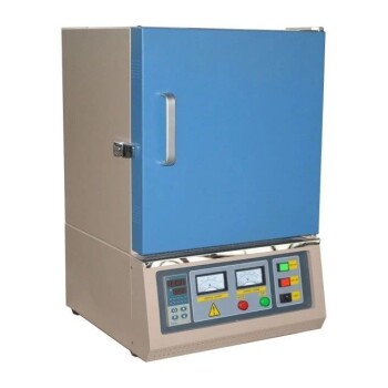
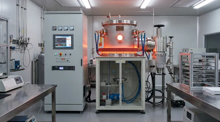
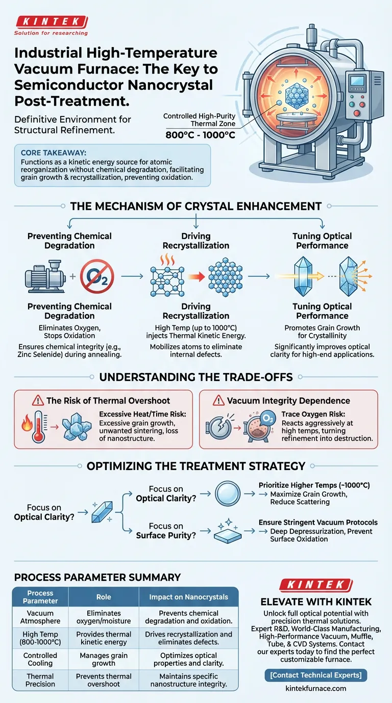
An industrial high-temperature vacuum furnace serves as the definitive environment for structural refinement in the post-treatment of semiconductor nanocrystals. It creates a controlled, high-purity thermal zone—typically operating between 800°C and 1000°C—that drives the transition from raw material to high-performance optical component.
Core Takeaway The furnace functions as a kinetic energy source that reorganizes atomic structures without chemical degradation. By combining high heat with a vacuum atmosphere, it facilitates necessary grain growth and recrystallization while strictly preventing the oxidation that would otherwise ruin the material's optical properties.
The Mechanism of Crystal Enhancement
Preventing Chemical Degradation
The primary challenge in treating semiconductor nanocrystals, such as zinc selenide, is their reactivity at high temperatures.
In a standard atmosphere, the heat required for treatment would cause immediate, uncontrolled oxidation. The vacuum furnace eliminates oxygen from the equation, ensuring the chemical integrity of the sample remains intact throughout long annealing cycles.
Driving Recrystallization
The furnace utilizes high temperatures (up to 1000°C) to inject thermal kinetic energy into the nanocrystals.
This energy mobilizes atoms within the material, allowing them to rearrange into a more ordered structure. This process, known as recrystallization, eliminates internal defects and stresses accumulated during earlier synthesis stages.
Tuning Optical Performance
The ultimate goal of this post-treatment is the enhancement of optical properties.
As the material recrystallizes, the process promotes grain growth. Larger, defect-free grains significantly improve the material's crystallinity. This structural perfection is directly responsible for the superior optical performance required in high-end semiconductor applications.
Understanding the Trade-offs
The Risk of Thermal Overshoot
While heat is necessary for ordering the crystal lattice, excessive thermal energy can be detrimental.
If the temperature exceeds the material's tolerance or the cycle is too long, you risk excessive grain growth or unwanted sintering. This can lead to a loss of the specific nanostructure characteristics you intended to preserve.
Vacuum Integrity Dependence
The success of the entire process hinges on the quality of the vacuum.
At 1000°C, even trace amounts of oxygen due to a minor leak or insufficient pump-down will react aggressively with the semiconductor material. This turns the furnace from a refinement tool into a destructive environment, potentially ruining the entire batch.
Optimizing the Treatment Strategy
To maximize the efficacy of the post-treatment process, align your furnace parameters with your specific material goals:
- If your primary focus is Optical Clarity: Prioritize higher temperatures (near 1000°C) to maximize grain growth and reduce scattering centers within the crystal lattice.
- If your primary focus is Surface Purity: Ensure your vacuum protocols are stringent, focusing on deep depressurization to prevent any surface oxidation during the annealing cycle.
The industrial vacuum furnace is not just a heater; it is a precision instrument for dictating the final quality and efficiency of semiconductor materials.
Summary Table:
| Process Parameter | Role in Post-Treatment | Impact on Nanocrystals |
|---|---|---|
| Vacuum Atmosphere | Eliminates oxygen/moisture | Prevents chemical degradation and oxidation |
| High Temp (800-1000°C) | Provides thermal kinetic energy | Drives recrystallization and eliminates defects |
| Controlled Cooling | Manages grain growth | Optimizes optical properties and clarity |
| Thermal Precision | Prevents thermal overshoot | Maintains specific nanostructure integrity |
Elevate Your Semiconductor Research with KINTEK
Unlock the full optical potential of your materials with KINTEK’s precision thermal solutions. Backed by expert R&D and world-class manufacturing, we provide high-performance Vacuum, Muffle, Tube, and CVD systems designed specifically for the rigorous demands of semiconductor post-treatment.
Whether you need strictly controlled atmospheres for grain growth or customizable high-temp furnaces for unique nanocrystal synthesis, KINTEK delivers the reliability your lab requires.
Ready to refine your process? Contact our technical experts today to find the perfect customizable furnace for your unique needs.
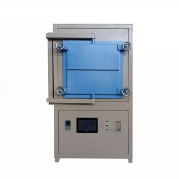
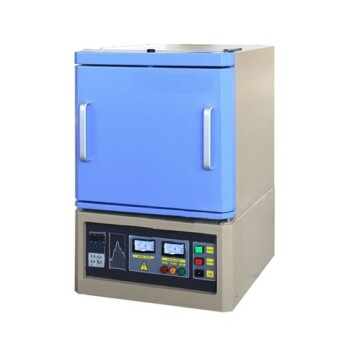
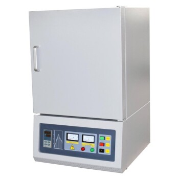
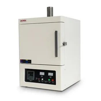
Visual Guide
References
- Aiman Akylbekovа, А. Usseinov. RAMAN ANALYSIS OF NANOCRYSTALS BASED ON ZINC SELENIDE. DOI: 10.52676/1729-7885-2023-4-77-84
This article is also based on technical information from Kintek Furnace Knowledge Base .
Related Products
- 2200 ℃ Tungsten Vacuum Heat Treat and Sintering Furnace
- 2200 ℃ Graphite Vacuum Heat Treat Furnace
- Molybdenum Vacuum Heat Treat Furnace
- 1400℃ Controlled Inert Nitrogen Atmosphere Furnace
- 1400℃ High Temperature Laboratory Tube Furnace with Alumina Tube
People Also Ask
- What core role does a high-temperature vacuum sintering furnace play in Sm:YAG ceramics? Mastering Optical Clarity
- What process conditions does a vacuum furnace provide for Yb:YAG ceramics? Expert Setup for Optical Purity
- What role does a high-temperature vacuum heat treatment furnace play in TBC post-processing? Enhance Coating Adhesion
- How does a tungsten-heated vacuum sintering furnace prepare (TbxY1-x)2O3 ceramics? Achieve 99%+ Density & Purity
- What are the benefits of using vacuum heat treating furnaces for metal alloys? Achieve Superior Metal Properties and Performance