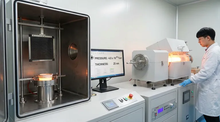
In the initial synthesis of Germanium-Carbon Cloth (GeCC), the thermal evaporation coating system serves as the foundational tool for catalyst deposition. Its primary function is to deposit a precise, 25-nanometer thick layer of tin (Sn) directly onto the carbon cloth substrate.
The system utilizes a vacuum environment to ensure tin particles are uniformly distributed and securely adhered to the carbon fibers. This creates the essential catalytic "seed" layer required to initiate and guide the subsequent growth of germanium nanowires.
The Mechanism of Deposition
Creating the Seed Layer
The thermal evaporation system is responsible for the very first step of material modification.
It targets the raw carbon cloth and introduces a tin (Sn) seed layer.
This layer is engineered to be approximately 25 nanometers thick, a specific gauge chosen to optimize the material for later stages of synthesis.
The Role of the Vacuum Environment
To achieve a high-quality coating, the system operates within a vacuum environment.
This controlled atmosphere eliminates air resistance and contaminants, allowing the evaporated tin particles to travel in a straight line to the substrate.
The result is a uniform and secure loading of particles onto the carbon fiber surface, which is critical for the structural integrity of the final interlayer.
The Strategic Purpose of the Tin Layer
Establishing Catalytic Sites
The deposited tin is not merely a passive coating; it plays an active chemical role.
These tin particles function as essential catalytic sites.
Without this specific seeding process, the carbon cloth would lack the necessary nucleation points required for complex nanostructure growth.
Enabling Directional Growth
The ultimate goal of this initial deposition is to prepare the substrate for the growth of germanium nanowires.
The tin seeds act as the template that dictates where these nanowires will sprout.
By ensuring the seeds are uniform, the system ensures the subsequent germanium growth is directional and organized, rather than random or chaotic.
Critical Considerations for Process Quality
Importance of Thickness Precision
The specific thickness of 25 nanometers is not arbitrary.
Deviations in this thickness could alter the size and density of the catalytic droplets.
If the layer is too thin or too thick, it may fail to support the optimal density of germanium nanowires in the next phase.
Adhesion and Stability
The "secure loading" mentioned in the process highlights the importance of substrate adhesion.
If the thermal evaporation settings are incorrect, the tin layer may delaminate or clump.
This would lead to a patchy distribution of germanium nanowires, compromising the performance of the final GeCC interlayer.
Making the Right Choice for Your Goal
To maximize the effectiveness of your synthesis process, prioritize the parameters of the evaporation system based on your specific requirements:
- If your primary focus is Nanowire Density: Ensure the thermal evaporation duration is strictly controlled to maintain the 25nm thickness, as this defines the catalyst particle size.
- If your primary focus is Structural Durability: Prioritize the vacuum quality during evaporation to guarantee the tin particles are securely bonded to the carbon fiber lattice.
The thermal evaporation system transforms plain carbon cloth into a reactive template, making the growth of advanced germanium nanostructures possible.
Summary Table:
| Process Parameter | Role in GeCC Synthesis | Impact on Final Product |
|---|---|---|
| Material Deposited | 25nm Tin (Sn) Layer | Creates essential catalytic nucleation sites |
| Environment | High-Vacuum Chamber | Ensures uniform particle distribution & adhesion |
| Substrate Type | Carbon Cloth | Serves as the base for germanium nanowire growth |
| Mechanism | Thermal Evaporation | Controls seed density for directional nanowire growth |
Elevate Your Material Research with KINTEK Precision
High-performance interlayers like GeCC demand absolute precision in deposition thickness and vacuum integrity. KINTEK provides industry-leading thermal evaporation and vacuum systems designed to meet the rigorous standards of advanced material synthesis.
Backed by expert R&D and manufacturing, KINTEK offers a comprehensive range of lab equipment including Muffle, Tube, Rotary, Vacuum, and CVD systems—all fully customizable to your specific research requirements. Whether you are establishing catalytic seed layers or scaling up nanowire production, our equipment ensures the stability and uniformity your project deserves.
Ready to optimize your synthesis process? Contact our technical specialists today to find the perfect thermal system for your laboratory.
References
- Syed Abdul Ahad, Hugh Geaney. Lithiophilic interlayer driven ‘bottom-up’ metal infilling in high current density Li-metal anodes. DOI: 10.1039/d4ta01072h
This article is also based on technical information from Kintek Furnace Knowledge Base .
Related Products
- HFCVD Machine System Equipment for Drawing Die Nano Diamond Coating
- RF PECVD System Radio Frequency Plasma Enhanced Chemical Vapor Deposition
People Also Ask
- What materials are commonly used in CVD coating systems? Explore Key Materials for Superior Coatings
- How can customers maximize the quality of CVD coatings? Master Pre-Coating Prep for Superior Results
- What is the function of high-purity Argon (Ar) gas during CVD? Optimize Your Thin Film Uniformity and Purity
- What is the advantage of using a CVD system for coating turbine blades? Master Complex Geometries with Ease
- What is Hot-filament Chemical Vapor Deposition (HFCVD)? Achieve High-Quality Thin Films with Precision Control

