At its core, Metal-Organic Chemical Vapor Deposition (MOCVD) is an industrial process used to grow high-purity, thin crystalline films on a substrate. It achieves this by introducing carefully controlled chemical vapors (precursors) into a reaction chamber. These vapors decompose upon contact with a heated surface, depositing a solid material one atomic layer at a time.
MOCVD is not merely a coating technique; it is a method for atomic-level construction. Its true value lies in the precise control it offers over material composition, enabling the creation of complex semiconductor structures that are the foundation of modern LEDs, lasers, and high-performance transistors.
The MOCVD Process: From Gas to Crystal
To understand how MOCVD works, it's best to break it down into the sequence of events that occur inside the reactor. Each step is meticulously controlled to ensure the final material has the desired properties.
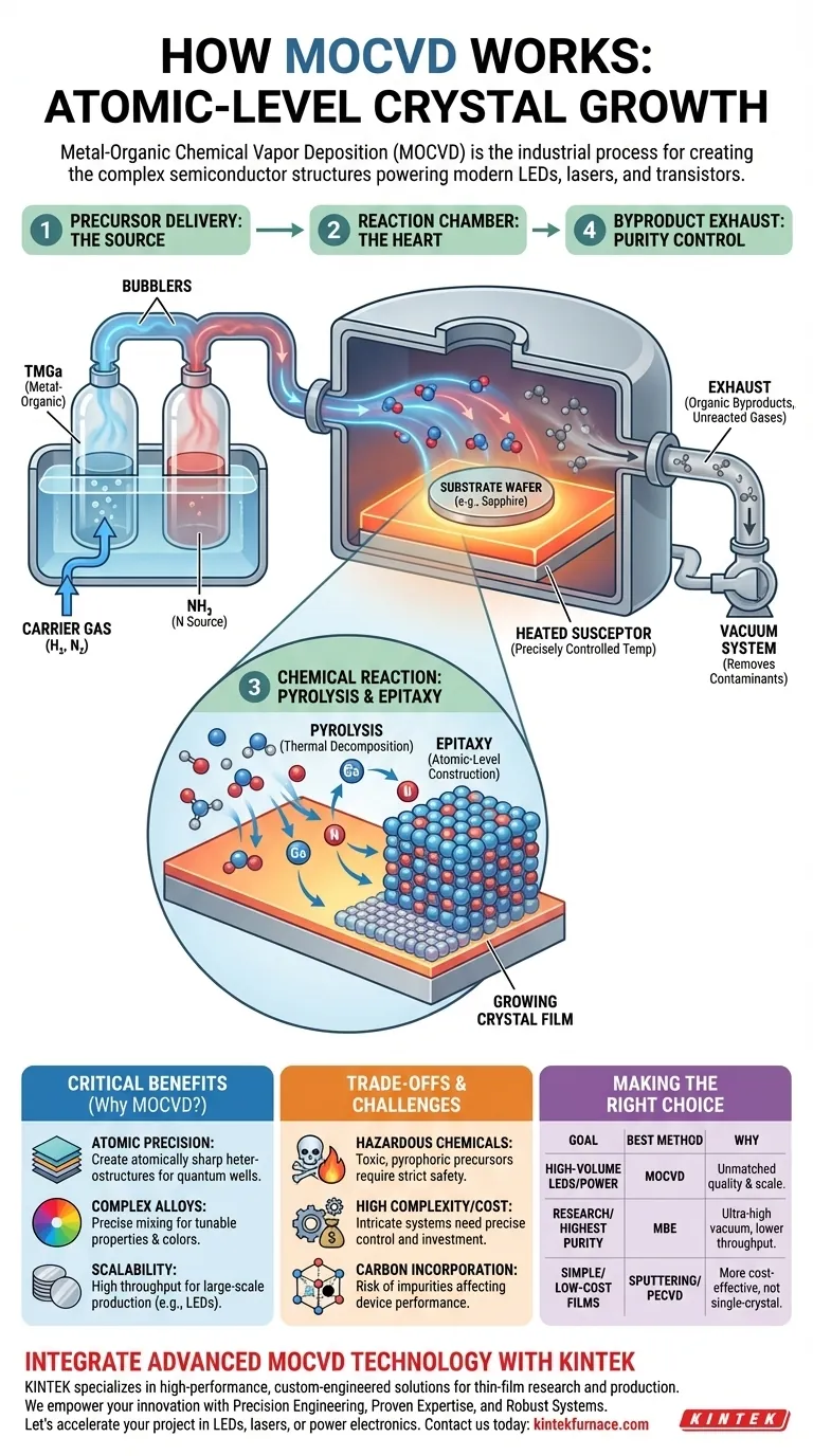
Precursor Delivery: The Source Materials
The process begins with the precursors, the chemical building blocks of the final film. These are "metal-organic" compounds, meaning they contain a metal atom (like Gallium, Aluminum, or Indium) chemically bonded to organic molecules.
These precursors, often volatile liquids or solids, are held in temperature-controlled cylinders called "bubblers." A highly pure carrier gas, typically hydrogen or nitrogen, is bubbled through the liquid (or over the solid) to pick up the precursor molecules and carry them in a vapor phase.
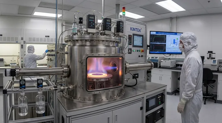
The Reaction Chamber: The Heart of the System
The mixture of carrier gas and precursor vapor is injected into a reaction chamber. Inside this chamber is a heated platform, known as a susceptor, which holds the substrate wafer (e.g., a disc of sapphire or silicon carbide).
The temperature of this substrate is the single most critical parameter in the process. It is precisely controlled, as it provides the energy needed to drive the chemical reaction.
The Chemical Reaction: Pyrolysis and Deposition
As the precursor gases flow across the hot substrate, they undergo pyrolysis—they thermally decompose. The high temperature breaks the chemical bonds holding the metal-organic molecules together.
This releases the desired metal atoms (like Gallium) onto the surface. At the same time, other precursors (like ammonia for nitrogen) also decompose. These freed atoms then migrate across the hot surface until they find an energetically favorable spot in the crystal lattice.
This growth process, where the new film copies the crystal structure of the underlying substrate, is called epitaxy. It is how MOCVD creates a perfect, single-crystal film rather than a disordered layer.
Byproduct Exhaust: Keeping it Pure
The leftover organic components and any unreacted gases are not part of the desired film. These chemical byproducts are continuously pumped out of the reaction chamber by a vacuum system. This exhaust process is crucial for preventing contamination and ensuring the purity of the growing crystal.
Why MOCVD is Critical for Modern Electronics
The true power of MOCVD is not just in growing one material, but in its ability to build complex, multi-layered structures with atomic precision.
Achieving Atomic Layer Precision
By simply opening and closing valves, operators can instantly switch which precursors are flowing into the chamber. This allows for the creation of heterostructures—stacks of different semiconductor materials—with atomically sharp interfaces. This capability is essential for creating the quantum wells that generate light in LEDs and lasers.
Engineering Complex Alloys
MOCVD allows for the precise mixing of multiple precursors simultaneously. For example, by flowing Trimethylgallium (TMGa) and Trimethylindium (TMIn) at the same time, one can grow an Indium Gallium Nitride (InGaN) alloy. The ratio of the gases directly controls the alloy's composition, which in turn determines its bandgap and the color of light it emits.
Scalability for Mass Production
While other ultra-high precision techniques exist, MOCVD is highly valued for its ability to handle large-diameter wafers and even multiple wafers in a single run. This high throughput makes it the dominant technology for the mass production of devices like LED lighting.
Understanding the Trade-offs and Challenges
While incredibly powerful, MOCVD is a complex and demanding process with significant trade-offs.
Hazardous Precursor Chemicals
The metal-organic precursors used in MOCVD are often highly toxic and pyrophoric, meaning they can ignite spontaneously on contact with air. This necessitates sophisticated gas handling cabinets and extensive safety protocols, adding to the cost and complexity of a facility.
High Cost and Complexity
MOCVD reactors are intricate machines that require precise, automated control over gas flow rates, temperature uniformity, and chamber pressure. The initial capital investment and ongoing maintenance costs are substantial.
The Problem of Carbon Incorporation
Because the precursors are "organic," there is an inherent risk that carbon atoms from the precursor molecules can be unintentionally incorporated into the growing crystal instead of being exhausted. This carbon acts as an impurity, creating defects that can harm the performance of the electronic device.
Making the Right Choice for Your Goal
The decision to use MOCVD is driven entirely by the material requirements of the final device.
- If your primary focus is high-volume production of LEDs, lasers, or power electronics: MOCVD is the industry standard due to its unmatched ability to grow high-quality compound semiconductors (like GaN and GaAs) at scale.
- If your primary focus is fundamental research requiring the absolute highest purity for exotic materials: You might consider Molecular Beam Epitaxy (MBE), which operates in an ultra-high vacuum and can offer purity advantages, though typically at a lower throughput.
- If your primary focus is simple, amorphous, or polycrystalline films: Far more cost-effective methods like sputtering, evaporation, or Plasma-Enhanced CVD (PECVD) are better suited for applications that do not require perfect single-crystal structures.
Ultimately, understanding the MOCVD process is key to appreciating how the invisible, atomic-level architecture of materials enables the technology we rely on every day.
Summary Table:
| Key MOCVD Stage | Purpose | Key Components |
|---|---|---|
| Precursor Delivery | Supplies chemical building blocks | Metal-organic compounds, bubblers, carrier gas |
| Reaction Chamber | Provides controlled environment for crystal growth | Heated susceptor, substrate wafer |
| Chemical Reaction | Decomposes precursors for atomic deposition | Pyrolysis, epitaxial growth |
| Byproduct Exhaust | Removes contaminants to ensure purity | Vacuum pump system |
Ready to Integrate Advanced MOCVD Technology into Your Lab?
KINTEK specializes in delivering high-performance, custom-engineered solutions for your most demanding thin-film research and production needs. Our expertise in advanced thermal systems, including MOCVD and PECVD, ensures you have the precise control required for growing high-purity semiconductor films.
We empower your innovation by providing:
- Precision Engineering: Tailored reactor components and heating systems for optimal film uniformity and composition control.
- Proven Expertise: Deep understanding of the thermal and chemical challenges inherent in processes like MOCVD.
- Robust & Reliable Systems: Durable equipment built for continuous operation in demanding R&D and production environments.
Let's discuss how our solutions can accelerate your project. Whether you are developing next-generation LEDs, laser diodes, or power electronics, KINTEK is your partner in advanced materials engineering.
Contact our experts today to explore how our high-temperature furnace and CVD system capabilities can be customized for your specific application.
Visual Guide
Related Products
- Cylindrical Resonator MPCVD Machine System for Lab Diamond Growth
- 915MHz MPCVD Diamond Machine Microwave Plasma Chemical Vapor Deposition System Reactor
- MPCVD Machine System Reactor Bell-jar Resonator for Lab and Diamond Growth
- Multi Heating Zones CVD Tube Furnace Machine for Chemical Vapor Deposition Equipment
- HFCVD Machine System Equipment for Drawing Die Nano Diamond Coating
People Also Ask
- What are future trends in MPCVD technology? Unlock Next-Gen Materials with AI and Efficiency
- How do carbon-containing groups contribute to diamond growth in the MPCVD method? Unlock High-Quality Diamond Synthesis
- What factors influence the quality of diamond deposition in the MPCVD method? Master the Critical Parameters for High-Quality Diamond Growth
- How does pressure affect the MPCVD growth process? Master Plasma Control for Superior Film Quality
- What are the key components of an MPCVD system? Unlock High-Purity Crystal Growth


