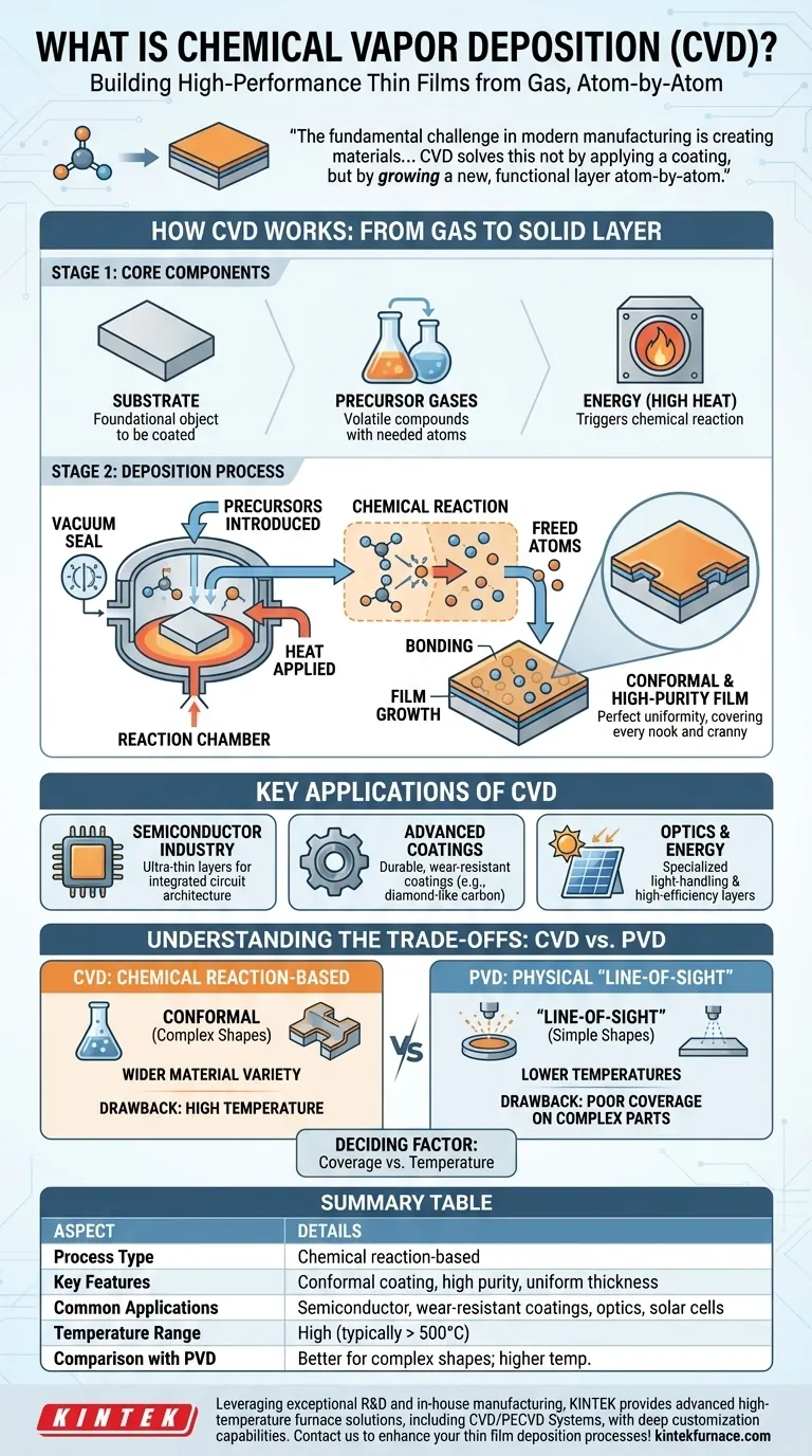
At its core, Chemical Vapor Deposition (CVD) is a sophisticated manufacturing process that builds a solid, high-performance thin film onto a surface from a gas. Precursor gases are introduced into a reaction chamber where they chemically react and deposit a new layer onto a target object, known as a substrate. This method is the foundation for producing critical components in the semiconductor industry and for creating advanced protective coatings.
The fundamental challenge in modern manufacturing is creating materials with perfect uniformity and specialized properties at a microscopic scale. CVD solves this not by applying a coating, but by growing a new, functional layer atom-by-atom directly onto a surface using controlled chemical reactions.
How CVD Works: From Gas to Solid Layer
CVD is less like painting and more like constructing a building one brick at a time. The process relies on a precise chemical reaction in a controlled environment to achieve its results.
The Core Components: Substrate, Precursors, and Energy
The process requires three key elements. The substrate is the foundational object that will be coated. Precursor gases are the volatile chemical compounds that contain the atoms needed for the new film. Finally, energy—most often in the form of high heat—is applied to trigger the chemical reaction.
The Deposition Process, Step-by-Step
First, a substrate is placed inside a vacuum reaction chamber. The precursor gases are then introduced into the chamber at a controlled rate.
As the chamber and substrate are heated to high temperatures, the energy causes the precursor gases to decompose or react with each other. This chemical reaction frees the desired solid material.
These newly freed atoms or molecules then deposit onto the surface of the warmer substrate, bonding with it and with each other. Over time, this builds up into a thin, solid film across the entire exposed surface.
The Result: A Conformal, High-Purity Film
Because the deposition happens from a gas phase that fills the entire chamber, CVD creates what is known as a conformal coating. This means the film is perfectly uniform in thickness, covering every nook, cranny, and complex feature of the substrate. The chemical nature of the process also results in exceptionally high-purity films.
Key Applications of CVD
The unique capabilities of CVD make it indispensable in industries where performance and precision are paramount.
The Semiconductor Industry
CVD is the workhorse of microchip manufacturing. It is used to deposit the ultra-thin layers of insulating, conducting, and semiconducting materials that form the intricate architecture of an integrated circuit.
Advanced Coatings
The process is used to apply extremely hard and durable coatings to tools and mechanical parts. These films, such as diamond-like carbon or titanium nitride, drastically increase resistance to wear, corrosion, and oxidation.
Optics and Energy
In optoelectronics, CVD is used to create specialized films with specific light-handling properties. It is also a key technology in producing the high-efficiency layers found in certain types of solar cells and other energy applications.
Understanding the Trade-offs: CVD vs. PVD
To fully grasp CVD's role, it's useful to compare it to the other primary thin-film technology: Physical Vapor Deposition (PVD).
CVD: Chemical Reaction-Based
CVD's strength lies in its ability to produce highly conformal and dense films on complex shapes. Because it's a chemical process, it can also be used to create a wider variety of compound materials. Its primary drawback is the high temperature required, which can damage sensitive substrates like plastics or certain metal alloys.
PVD: Physical "Line-of-Sight" Deposition
PVD works by physically bombarding a solid target to vaporize it (sputtering) or by simply boiling it (evaporation). This vapor then travels in a straight line and condenses on the substrate. This "line-of-sight" nature means it struggles to coat complex, non-flat surfaces uniformly. However, PVD processes typically run at much lower temperatures than CVD.
The Deciding Factor: Coverage vs. Temperature
The choice between CVD and PVD often comes down to a simple trade-off. If you need a perfect, uniform coating on a complex 3D part and the part can withstand the heat, CVD is superior. If your part has a simple geometry or cannot tolerate high temperatures, PVD is often the more practical choice.
Making the Right Choice for Your Goal
Selecting the correct deposition technology depends entirely on the material requirements and the nature of the substrate.
- If your primary focus is creating the complex, layered architecture of a semiconductor: CVD is the industry standard due to its ability to deposit highly pure, conformal films.
- If your primary focus is applying a wear-resistant coating to a simple-shaped cutting tool: PVD is often a more cost-effective and lower-temperature alternative.
- If your primary focus is uniformly coating a complex 3D part for corrosion protection: CVD's conformal nature makes it the superior choice, provided the part can handle the heat.
Ultimately, understanding whether your application requires chemical growth or physical deposition is the key to creating high-performance surfaces.
Summary Table:
| Aspect | Details |
|---|---|
| Process Type | Chemical reaction-based thin film deposition |
| Key Features | Conformal coating, high purity, uniform thickness |
| Common Applications | Semiconductor manufacturing, wear-resistant coatings, optics, solar cells |
| Temperature Range | High temperatures (typically above 500°C) |
| Comparison with PVD | Better for complex shapes; higher temperature than PVD |
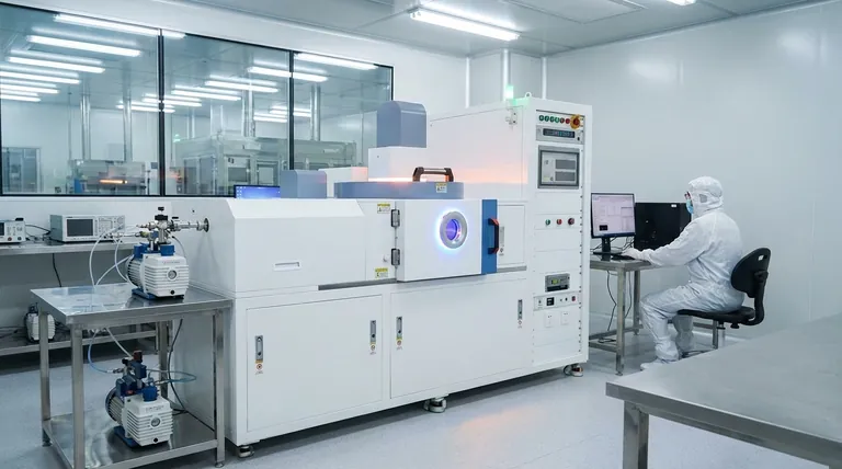
Leveraging exceptional R&D and in-house manufacturing, KINTEK provides diverse laboratories with advanced high-temperature furnace solutions. Our product line, including Muffle, Tube, Rotary Furnaces, Vacuum & Atmosphere Furnaces, and CVD/PECVD Systems, is complemented by our strong deep customization capability to precisely meet unique experimental requirements. Contact us today to enhance your thin film deposition processes with tailored, high-performance solutions!
Visual Guide
Related Products
- HFCVD Machine System Equipment for Drawing Die Nano Diamond Coating
- Cylindrical Resonator MPCVD Machine System for Lab Diamond Growth
- Custom Made Versatile CVD Tube Furnace Chemical Vapor Deposition CVD Equipment Machine
- 915MHz MPCVD Diamond Machine Microwave Plasma Chemical Vapor Deposition System Reactor
- RF PECVD System Radio Frequency Plasma Enhanced Chemical Vapor Deposition
People Also Ask
- What is chemical vapor deposition (CVD) and its primary industrial application? Unlock Precision Thin Films for Electronics
- How can customers maximize the quality of CVD coatings? Master Pre-Coating Prep for Superior Results
- What is the function of high-purity Argon (Ar) gas during CVD? Optimize Your Thin Film Uniformity and Purity
- What core function does CVD equipment serve in h-BN anti-corrosion? Master Precision Synthesis for High-Performance Films
- What is the advantage of using a CVD system for coating turbine blades? Master Complex Geometries with Ease