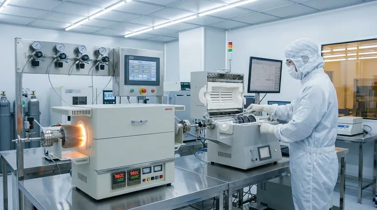
In the semiconductor industry, vacuum furnaces are specialized chambers used to perform critical high-temperature processes like annealing, sintering, and film deposition on silicon wafers. By removing air and other reactive gases, these furnaces create an ultra-pure, precisely controlled environment that is essential for fabricating high-performance, reliable microelectronic components.
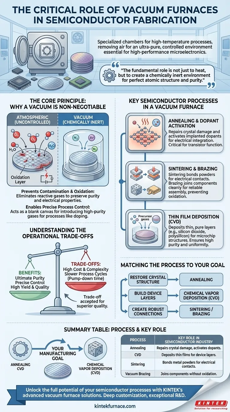
The fundamental role of a vacuum furnace is not just to heat materials, but to create a chemically inert environment. This absolute control over the processing atmosphere is what enables the creation of semiconductor materials with the perfect atomic structure and purity required for modern electronics.
The Core Principle: Why a Vacuum is Non-Negotiable
The fabrication of a semiconductor device involves manipulating materials at an atomic level. The presence of uncontrolled atmospheric gases, especially oxygen, can introduce catastrophic defects that render a device useless. A vacuum environment is the foundational tool for eliminating this risk.
Preventing Contamination and Oxidation
Even trace amounts of oxygen or water vapor can react with a silicon wafer at high temperatures, forming an unwanted silicon dioxide layer. This uncontrolled oxidation disrupts the electrical properties of the device.
A vacuum furnace evacuates these reactive gases, creating a chemically inert space. This prevents unwanted reactions and ensures the material's purity and intended electrical characteristics are preserved.
Enabling Precise Process Control
Once a vacuum is established, engineers can introduce specific, high-purity gases in precise amounts. This allows for processes like doping, where controlled impurities are intentionally introduced to alter the silicon's conductivity.
This level of atmospheric control is impossible in a non-vacuum environment. The vacuum acts as a perfect blank canvas, upon which specific chemical processes can be executed with extreme precision.
Key Semiconductor Processes in a Vacuum Furnace
Different stages of chip manufacturing rely on the unique capabilities of vacuum furnaces. These processes modify the wafer's properties, build new layers, or prepare it for assembly.
Annealing and Dopant Activation
Annealing is a heat treatment process that repairs damage to the crystal lattice of the silicon wafer, which can occur during steps like ion implantation.
This process must be conducted in an oxygen-free environment to prevent contamination. It "activates" the implanted dopant atoms, allowing them to become electrically integrated into the silicon crystal, which is critical for transistor function.
Sintering and Brazing
Sintering is used to heat compacted materials (like metal powders) below their melting point, causing the particles to bond together and increase the material's strength and conductivity. This is vital for forming reliable electrical contacts on the chip.
Vacuum brazing is a method for joining components together, such as attaching the semiconductor die to its packaging. The vacuum prevents oxidation on the joint surfaces, ensuring a strong, clean, and reliable connection.
Thin Film Deposition
Many vacuum furnaces are configured for Chemical Vapor Deposition (CVD). In this process, precursor gases are introduced into the chamber where they react and deposit a thin, solid film onto the wafer.
CVD is used to build up the layers of a microchip, such as silicon dioxide (for insulation), silicon nitride (for protection), or polysilicon (for transistor gates). The vacuum ensures these films are deposited with high purity and uniformity.
Understanding the Operational Trade-offs
While indispensable, using vacuum furnaces involves clear trade-offs. The pursuit of ultimate purity and control comes at the cost of complexity and speed.
High Cost and Complexity
Vacuum systems, including the pumps, seals, and monitoring equipment, are significantly more complex and expensive to purchase and maintain than standard atmospheric furnaces. Specialized furnaces are often required for different temperature ranges and processes, further increasing costs.
Slower Process Cycles
Achieving a high-quality vacuum takes time. The pump-down cycle to evacuate the chamber before processing and the controlled backfill and cooling cycles afterward make the overall process time much longer than for atmospheric heating.
This trade-off is accepted because the quality and yield improvements for sensitive semiconductor devices far outweigh the cost of the slower cycle time. There is simply no other way to achieve the required level of environmental purity.
Matching the Process to Your Goal
The specific vacuum process you use depends entirely on the manufacturing outcome you need to achieve.
- If your primary focus is restoring crystal structure or activating electrical properties: Your key process is annealing, which requires a clean, oxygen-free heat treatment.
- If your primary focus is building the layers of a device: You will rely on Chemical Vapor Deposition (CVD) to uniformly deposit pure films like oxides or polysilicon.
- If your primary focus is creating robust connections or assembling components: You will use sintering to form electrical contacts or brazing for die attachment in a contamination-free environment.
Ultimately, mastering the vacuum environment is fundamental to mastering the fabrication of any advanced semiconductor device.
Summary Table:
| Process | Key Role in Semiconductor Industry |
|---|---|
| Annealing | Repairs crystal damage and activates dopants in silicon wafers. |
| Chemical Vapor Deposition (CVD) | Deposits thin films (e.g., silicon dioxide, polysilicon) for device layers. |
| Sintering | Bonds metal powders to form strong electrical contacts. |
| Vacuum Brazing | Joins components without oxidation for reliable assembly. |
Unlock the full potential of your semiconductor processes with KINTEK's advanced vacuum furnace solutions. Leveraging exceptional R&D and in-house manufacturing, we provide diverse laboratories with high-temperature furnace options like Muffle, Tube, Rotary, Vacuum & Atmosphere Furnaces, and CVD/PECVD Systems. Our strong deep customization capability ensures precise alignment with your unique experimental needs, enhancing purity, control, and yield. Contact us today to discuss how we can support your high-performance microelectronics fabrication!
Visual Guide
Related Products
- 600T Vacuum Induction Hot Press Vacuum Heat Treat and Sintering Furnace
- Vacuum Hot Press Furnace Machine Heated Vacuum Press
- 2200 ℃ Tungsten Vacuum Heat Treat and Sintering Furnace
- Vacuum Hot Press Furnace Machine Heated Vacuum Press Tube Furnace
- Vacuum Heat Treat Furnace with Ceramic Fiber Liner
People Also Ask
- What are the key advantages of vacuum hot press sintering furnaces? Achieve Superior Density and Purity in Materials
- What are the advantages of using a vacuum hot press sintering furnace for preparing high-density carbon nanotube reinforced copper matrix composites? Achieve Maximum Density and Purity for Superior Performance
- What are the benefits of using a vacuum hot press sintering furnace for the preparation of SiCw/2024 aluminum matrix composites? Achieve High-Performance Aerospace Materials
- What is the core function of a vacuum hot press sintering furnace in the preparation of high-density RuTi alloys? Achieve Maximum Density and Purity
- How does the vacuum environment in a vacuum hot press sintering furnace protect chromium-containing ceramics? Find out.


