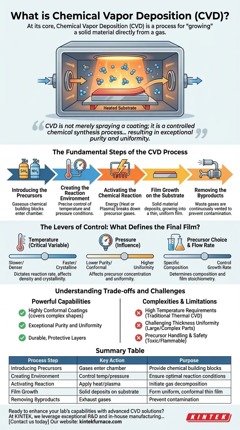
At its core, Chemical Vapor Deposition (CVD) is a process for "growing" a solid material directly from a gas. It involves introducing one or more gaseous chemical compounds, known as precursors, into a chamber containing the object to be coated (the substrate). By applying energy—typically heat—these gases react and decompose, and the resulting solid material deposits onto the substrate, forming a new, high-quality thin film.
CVD is not merely spraying a coating; it is a controlled chemical synthesis process. Gaseous ingredients are carefully chosen and activated to build a solid film, often atom by atom, directly onto a substrate's surface, resulting in exceptional purity and uniformity.
The Fundamental Steps of the CVD Process
To truly understand CVD, it's best to think of it as a multi-stage manufacturing process occurring inside a controlled reaction chamber. Each stage is a lever that can be adjusted to define the final film's properties.
1. Introducing the Precursors
The process begins by introducing precursor gases into the reaction chamber. These gases are the chemical "building blocks" that contain the elements required for the final film. For example, to create a silicon nitride film, precursors like silane (SiH₄) and ammonia (NH₃) might be used.
2. Creating the Reaction Environment
The substrate is placed inside a reaction chamber where conditions like temperature and pressure are precisely controlled. This controlled environment is critical for ensuring the chemical reactions happen as intended and that impurities are minimized.
3. Activating the Chemical Reaction
Energy is supplied to the system to break down the precursor gases and initiate the chemical reaction. The most common method is heat (Thermal CVD), where the chamber is heated to hundreds or even thousands of degrees Celsius. This thermal energy gives the gas molecules enough energy to react when they contact the hot substrate surface.
Other energy sources, like plasma (in Plasma-Enhanced CVD, or PECVD), can also be used. Plasma allows the reactions to occur at much lower temperatures, making it suitable for coating heat-sensitive materials.
4. Film Growth on the Substrate
As the energized precursors react on or near the substrate, a new solid material is formed. This solid product deposits directly onto the substrate surface, growing into a thin, uniform film. Because the precursors are in a gaseous state, they can reach all exposed areas, allowing CVD to produce highly conformal coatings that cover even complex, non-flat shapes.
5. Removing the Byproducts
The chemical reactions that form the solid film also create gaseous byproducts. These waste gases are continuously removed from the reaction chamber by a vacuum or exhaust system to prevent them from contaminating the film or interfering with the deposition process.
The Levers of Control: What Defines the Final Film?
The quality, thickness, and composition of the deposited film are not accidental. They are the direct result of carefully manipulating several key parameters during the process.
The Role of Temperature
Temperature is arguably the most critical variable. It dictates the rate of the chemical reactions. Higher temperatures generally lead to faster deposition rates and can result in denser, more crystalline films. However, the temperature must be compatible with the substrate material.
The Impact of Pressure
The pressure inside the chamber influences the concentration of precursor molecules and how they travel. Lower pressures can increase the purity of the film by reducing the chance of unwanted gas-phase reactions and improving the uniformity of the coating across the substrate.
Precursor Choice and Flow Rate
The specific precursors chosen determine the chemical composition of the final film. The rate at which these gases are flowed into the chamber directly affects the growth rate of the film and can be used to control its stoichiometry (the ratio of elements).
Understanding the Trade-offs and Challenges
While powerful, CVD is not without its complexities and limitations. An objective assessment requires understanding these factors.
High Temperature Requirements
Traditional Thermal CVD often requires very high temperatures. This makes it unsuitable for substrates that can melt, warp, or degrade under heat, such as plastics or certain electronic components. This limitation is what drives the use of alternative methods like PECVD.
Conformal Coating vs. Uniformity
While CVD is excellent at creating conformal coatings, achieving perfect thickness uniformity across a large or complex part can be challenging. Gas flow dynamics and temperature gradients within the chamber can cause the film to grow thicker in some areas than others.
Precursor Handling and Safety
Many precursors used in CVD are highly toxic, flammable, or corrosive. This necessitates sophisticated handling procedures, safety monitoring, and exhaust treatment systems, which adds to the cost and complexity of the operation.
How to Apply This to Your Project
Your choice to use CVD, and which variant to use, should be guided by the specific goal you need to achieve.
- If your primary focus is creating highly pure, dense films for electronics: The precise control over composition and structure offered by CVD is ideal for semiconductor manufacturing.
- If your primary focus is coating temperature-sensitive substrates: You should investigate lower-temperature variants like Plasma-Enhanced CVD (PECVD) to avoid damaging your parts.
- If your primary focus is applying a durable, protective layer: CVD excels at creating hard, non-porous coatings that protect parts from wear, corrosion, and high-temperature oxidation.
By understanding these core principles, you can effectively leverage CVD as a precise materials synthesis tool rather than just a simple coating technique.
Summary Table:
| Process Step | Key Action | Purpose |
|---|---|---|
| Introducing Precursors | Gases enter chamber | Provide chemical building blocks |
| Creating Environment | Control temp/pressure | Ensure optimal reaction conditions |
| Activating Reaction | Apply heat/plasma | Initiate gas decomposition |
| Film Growth | Solid deposits on substrate | Form uniform, conformal thin film |
| Removing Byproducts | Exhaust gases | Prevent contamination |
Ready to enhance your lab's capabilities with advanced CVD solutions? At KINTEK, we leverage exceptional R&D and in-house manufacturing to provide high-temperature furnaces like CVD/PECVD Systems, tailored to your unique needs. Whether you're in electronics, materials science, or protective coatings, our deep customization ensures precise performance. Contact us today to discuss how our expertise can drive your project forward!
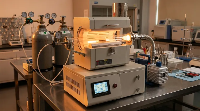
Visual Guide
Related Products
- Custom Made Versatile CVD Tube Furnace Chemical Vapor Deposition CVD Equipment Machine
- MPCVD Machine System Reactor Bell-jar Resonator for Lab and Diamond Growth
- Multi Heating Zones CVD Tube Furnace Machine for Chemical Vapor Deposition Equipment
- 915MHz MPCVD Diamond Machine Microwave Plasma Chemical Vapor Deposition System Reactor
- Slide PECVD Tube Furnace with Liquid Gasifier PECVD Machine
People Also Ask
- What customization options are available for CVD tube furnaces? Tailor Your System for Superior Material Synthesis
- What temperature range do standard CVD tube furnaces operate at? Unlock Precision for Your Material Deposition
- How might AI and machine learning enhance CVD tube furnace processes? Boost Quality, Speed, and Safety
- What improvements can be made to the bonding force of gate dielectric films using a CVD tube furnace? Enhance Adhesion for Reliable Devices
- Which industries and research fields benefit from CVD tube furnace sintering systems for 2D materials? Unlock Next-Gen Tech Innovations


