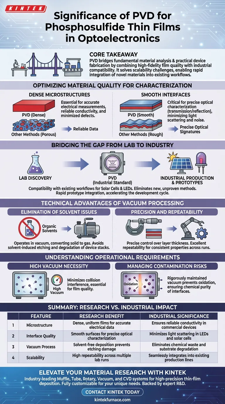
The primary significance of Physical Vapor Deposition (PVD) lies in its unique ability to bridge the gap between fundamental material analysis and practical device fabrication. PVD produces phosphosulfide thin films with the dense microstructures and smooth interfaces necessary for accurate electrical and optical characterization. Furthermore, because PVD is an industrial standard, it allows novel semiconductor materials to be rapidly integrated into existing processing flows for solar cell and LED prototypes.
Core Takeaway PVD methods solve the critical challenge of scalability by combining high-fidelity film quality with industrial compatibility. By eliminating organic solvents and ensuring interface purity, PVD allows researchers to validate materials in the lab and immediately apply them to practical optoelectronic manufacturing workflows.
Optimizing Material Quality for Characterization
Achieving Dense Microstructures
For phosphosulfide materials to be viable in electronics, the film must be uniform and solid. PVD produces dense microstructures, which are superior to the porous structures often resulting from other methods.
This structural density is vital for obtaining accurate electrical measurements. It ensures reliable conductivity and minimizes the defects that can skew performance data during the research phase.
Ensuring Smooth Interfaces
PVD creates exceptionally smooth interfaces between film layers. Rough surfaces can scatter light, introducing noise into optical data.
Smoothness is critical for optical characterization, specifically transmission and reflection spectroscopy. High-quality interfaces allow researchers to capture precise optical signatures without interference from surface irregularities.
Bridging the Gap from Lab to Industry
Compatibility with Industrial Workflows
A major hurdle in materials science is transferring a lab discovery to a production line. PVD is already an industrial-grade technique widely used in commercial manufacturing.
This compatibility means that phosphosulfide materials developed in the laboratory do not require new, unproven fabrication methods to be scaled up. They fit seamlessly into existing processing flows for devices like solar cells and LEDs.
Rapid Prototype Integration
Because the fabrication method is consistent with industry standards, the time between material synthesis and device testing is reduced.
PVD allows semiconductor materials to be rapidly integrated into functional optoelectronic conversion devices. This accelerates the development cycle from raw material research to working prototypes.
Technical Advantages of Vacuum Processing
Elimination of Solvent Issues
Unlike liquid-based processing, PVD operates in a vacuum and converts solid precursors directly to gas. This eliminates the need for organic solvents.
By removing solvents, researchers avoid solvent-induced etching problems that can degrade the substrate or underlying layers, preserving the integrity of the device stack.
Precision and Repeatability
PVD systems allow for precise control over the thickness of each thin-film layer. This is essential for optoelectronics, where performance often depends on specific layer geometries.
The process also offers excellent repeatability, ensuring that successful film properties can be duplicated consistently across multiple fabrication runs.
Understanding the Operational Requirements
The Necessity of High Vacuum
To achieve these results, PVD relies heavily on maintaining a high-vacuum environment. This is not merely for cleanliness; it is a fundamental requirement to minimize collision interference between residual air molecules and the deposited ions.
Managing Contamination Risks
While PVD reduces external impurities, the system must be rigorously maintained. The vacuum is the only barrier preventing oxidation contamination during film formation.
Any breach in the vacuum integrity can introduce impurities that compromise the chemical purity of the deposition interfaces. Therefore, the quality of the film is strictly bound to the quality of the vacuum environment.
Making the Right Choice for Your Goal
PVD offers a distinct pathway for researchers looking to validate phosphosulfide materials for real-world applications.
- If your primary focus is Fundamental Characterization: PVD provides the dense, smooth films required to obtain noise-free electrical and optical data.
- If your primary focus is Device Prototyping: PVD ensures your fabrication process is compatible with industrial standards, allowing for immediate integration into solar or LED architectures.
- If your primary focus is Layer Integrity: PVD eliminates solvent-related damage and provides the thickness control needed for complex, multi-layered stacks.
Ultimately, choosing PVD validates your material not just as a scientific curiosity, but as a viable candidate for scalable optoelectronic technology.
Summary Table:
| Feature | Research Benefit | Industrial Significance |
|---|---|---|
| Microstructure | Dense, uniform films for accurate electrical data | Ensures reliable conductivity in commercial devices |
| Interface Quality | Smooth surfaces for precise optical characterization | Minimizes light scattering in LEDs and solar cells |
| Vacuum Process | Solvent-free deposition prevents etching damage | Eliminates chemical waste and substrate degradation |
| Scalability | High repeatability across multiple lab runs | Seamlessly integrates into existing production lines |
Elevate Your Material Research with KINTEK
Transitioning from lab discovery to industrial reality requires high-precision equipment. KINTEK provides industry-leading Muffle, Tube, Rotary, Vacuum, and CVD systems, specifically engineered to help you achieve the vacuum integrity and layer precision needed for next-generation optoelectronics.
Backed by expert R&D and world-class manufacturing, our systems are fully customizable to meet your unique thin-film deposition and high-temperature processing needs. Don't let fabrication limitations slow down your innovation.
Contact KINTEK today to discuss your custom solution
Visual Guide
References
- Lena Angelika Mittmann, Andrea Crovetto. Phosphosulfide semiconductors for optoelectronics and solar energy conversion. DOI: 10.1088/2515-7639/ad3aa3
This article is also based on technical information from Kintek Furnace Knowledge Base .
Related Products
- RF PECVD System Radio Frequency Plasma Enhanced Chemical Vapor Deposition
- HFCVD Machine System Equipment for Drawing Die Nano Diamond Coating
- MPCVD Machine System Reactor Bell-jar Resonator for Lab and Diamond Growth
- 915MHz MPCVD Diamond Machine Microwave Plasma Chemical Vapor Deposition System Reactor
- Slide PECVD Tube Furnace with Liquid Gasifier PECVD Machine
People Also Ask
- What are the applications of plasma enhanced chemical vapor deposition? Key Uses in Electronics, Optics & Materials
- What are the key advantages of PECVD technology? Achieve Low-Temperature, High-Quality Thin Film Deposition
- What are the system specifications of the PECVD system? Unlock Precision Thin-Film Deposition
- What are some promising applications of PECVD-prepared 2D materials? Unlock Advanced Sensing and Optoelectronics
- How are deposition rates and film properties controlled in PECVD? Master Key Parameters for Optimal Thin Films


