Silver paste coating and high-temperature curing are the essential processes used to create a high-performance electrode layer on ceramic surfaces. This layer acts as the physical bridge between the ceramic sample and precision measuring instruments such as LCR meters and impedance analyzers. Without this conductive interface, it is impossible to accurately evaluate a material’s dielectric constant, impedance, or ferroelectric behavior.
The core significance of this process lies in the transformation of a liquid conductive suspension into a solid, low-resistance ohmic contact. This ensures uniform electric field distribution and stable signal transmission, which are the fundamental requirements for reliable electrical characterization in material science.
The Role of Silver Paste in Electrode Fabrication
Establishing the Physical Interface
Ceramic materials are often insulators or semiconductors that cannot be directly connected to testing leads. Silver paste is applied to two parallel surfaces of a sample to prepare the physical foundation for an electrode.
Achieving Material Compatibility
High-purity silver paste is chosen for its excellent conductivity and its ability to adhere to complex ceramic oxides, such as Ba0.85Ca0.15Zr0.1Ti0.9O3 (BCZT). This ensures that the electrical signals measured reflect the properties of the ceramic itself rather than a poor connection.
The Mechanism of High-Temperature Curing
Solvent Evaporation and Pre-drying
The process typically begins with a low-temperature phase, often around 130°C, to remove organic solvents. This step is a prerequisite for ensuring that the silver particles can eventually adhere tightly to the ceramic substrate without bubbling or cracking.
Sintering and Ohmic Contact Formation
High-temperature curing, often conducted at 600°C, sinters the silver particles into a continuous, durable conductive layer. This heat treatment is critical for establishing a robust ohmic contact, which minimizes resistance at the interface between the metal and the ceramic.
Impact on Measurement Integrity
Minimizing Contact Resistance
A properly cured silver electrode minimizes parasitic resistance that could otherwise skew data. This allows for the accurate acquisition of core parameters like capacitance and dielectric loss across a wide range of frequencies and temperatures.
Ensuring Uniform Electric Field Distribution
The cured silver layer ensures that the electric field is uniformly distributed across the entire volume of the sample. This uniformity is essential for obtaining precise measurements of temperature-dependent electrical properties and ionic conductivity.
Stabilizing Signal Transmission
By creating a permanent, sintered bond, the curing process provides a stable signal transmission path. This stability is vital when performing Electrochemical Impedance Spectroscopy (EIS) or testing ferroelectric systems where signal noise must be kept to a minimum.
Understanding the Trade-offs and Pitfalls
Thermal Expansion Mismatch
If the heating or cooling rate during curing is too rapid, the difference in the coefficient of thermal expansion between the silver and the ceramic can cause the electrode to delaminate. Gradual temperature ramping is usually required to maintain structural integrity.
Over-Sintering and Diffusion
Curing at temperatures significantly higher than recommended can lead to unwanted silver diffusion into the ceramic bulk. This can alter the chemical composition of the sample and lead to inaccurate electrical readings or internal short circuits.
Surface Contamination
Any residual oils or dust on the ceramic surface prior to coating will prevent the silver from bonding correctly. Proper surface preparation is just as important as the curing temperature for ensuring a low-resistance contact.
How to Apply This to Your Project
When preparing ceramic samples for electrical characterization, your approach should be dictated by your specific testing requirements:
- If your primary focus is high-precision dielectric testing: Ensure you use a specialized electrode firing furnace at 600°C to achieve the most stable ohmic contact possible.
- If your primary focus is ionic conductivity (EIS): Prioritize a thorough pre-drying phase at 130°C to remove all organic solvents, ensuring a uniform electrical signal through the sample.
- If your primary focus is characterizing new ferroelectric compositions: Use high-purity silver paste and verify the uniformity of the coating thickness to ensure a consistent electric field during high-voltage testing.
Executing these steps with precision ensures that your experimental data is a true reflection of the material's properties rather than an artifact of poor electrode preparation.
Summary Table:
| Process Stage | Typical Temperature | Key Function | Benefit to Electrical Testing |
|---|---|---|---|
| Pre-drying | ~130°C | Organic solvent evaporation | Prevents electrode bubbling and cracking |
| Sintering/Curing | ~600°C | Ohmic contact formation | Minimizes parasitic resistance for accurate data |
| Electrode Sintering | High Temperature | Continuous silver layer | Ensures uniform electric field distribution |
| Cooling | Controlled Rate | Stress management | Prevents delamination due to thermal expansion |
Optimize Your Material Characterization with KINTEK
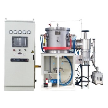
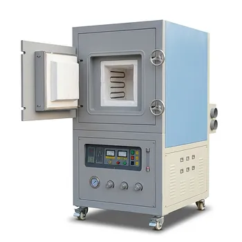
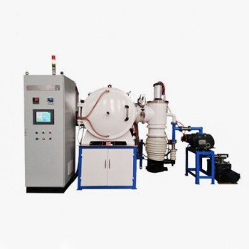
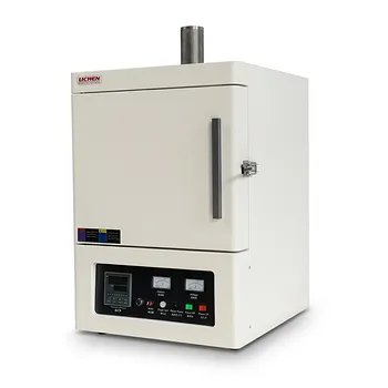
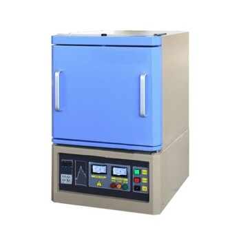
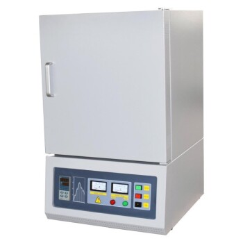
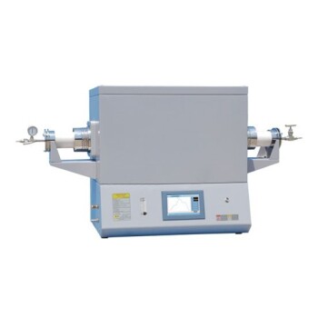
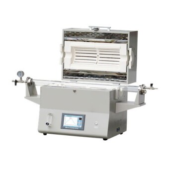
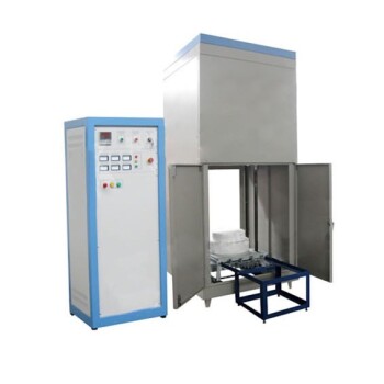
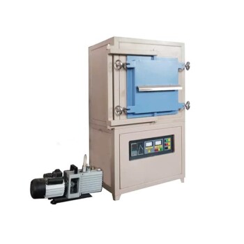
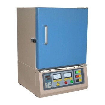
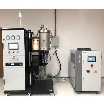
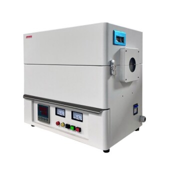
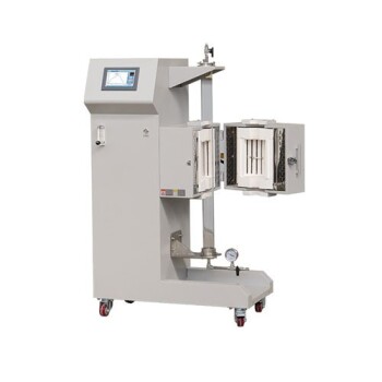
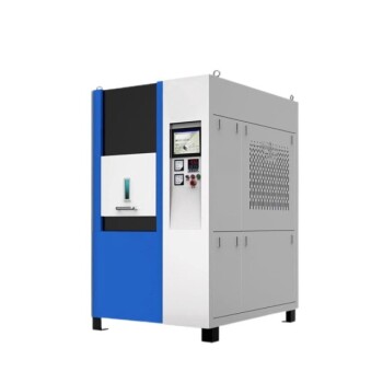
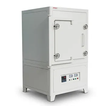
Precision in electrical testing starts with flawless electrode preparation. KINTEK specializes in advanced laboratory equipment designed to meet the rigorous demands of material science. Our comprehensive range of high-temperature furnaces—including muffle, tube, rotary, vacuum, CVD, and atmosphere furnaces—provides the stable thermal environments necessary for perfect silver paste sintering and ohmic contact formation.
Whether you are characterizing new ferroelectrics or conducting complex impedance spectroscopy, our customizable solutions ensure uniform heating and precise temperature control.
Ready to elevate your research accuracy? Contact our experts today to find the perfect furnace for your ceramic testing and laboratory needs!
References
- Sami Ullah Khan, Yaseen Iqbal. Dielectric, impedance, and energy storage properties of Bi(Mg <sub>0.5</sub> Sn <sub>0.5</sub> )O <sub>3</sub> modified Bi <sub>0.5</sub> Na <sub>0.5</sub> TiO <sub>3</sub> based ceramics. DOI: 10.1111/ijac.15030
This article is also based on technical information from Kintek Furnace Knowledge Base .
Related Products
- 2200 ℃ Tungsten Vacuum Heat Treat and Sintering Furnace
- High Temperature Muffle Oven Furnace for Laboratory Debinding and Pre Sintering
- 2200 ℃ Graphite Vacuum Heat Treat Furnace
- 1200℃ Muffle Oven Furnace for Laboratory
- 1800℃ High Temperature Muffle Oven Furnace for Laboratory
People Also Ask
- How does a tungsten-heated vacuum sintering furnace prepare (TbxY1-x)2O3 ceramics? Achieve 99%+ Density & Purity
- What wear-resistance enhancements are achieved by powder coating? The Role of Vacuum Sintering Furnaces
- How do compaction pressure and vacuum sintering optimize porous ceramics? Maximize Density & Toughness
- What role does a high-temperature vacuum sintering furnace play in the densification of WC-10(Ni, Ni/Co) alloys?
- What core role does a high-temperature vacuum sintering furnace play in Sm:YAG ceramics? Mastering Optical Clarity