The primary purpose of vacuum sputtering systems in this context is to create the critical conductive interface between the device's piezoelectric material and its power source. Specifically, these systems deposit highly conductive metal thin films, such as platinum, onto crystallized PZT surfaces to form high-quality electrodes.
The core function of this technology is to transform a raw piezoelectric material into a functional transducer. by precisely controlling the deposition process, the system ensures the electrode has the exact thickness and adhesion necessary to efficiently convert electrical signals into the mechanical vibrations used for haptic feedback.

Achieving Precision in Metal Deposition
Creating Highly Conductive Films
Vacuum sputtering is utilized to deposit specific metals that serve as the electrical pathway for the device.
In high-performance haptics, platinum is frequently used due to its excellent conductivity and stability. This metal is deposited directly onto the surface of crystallized PZT (lead zirconate titanate) thin films.
Controlling Thickness and Adhesion
The effectiveness of a haptic device relies on the physical integrity of the electrode layer.
By meticulously adjusting the sputtering power and duration, manufacturers can dictate the exact thickness of the film. This process control is also vital for ensuring strong adhesion, preventing the electrode from delaminating during operation.
Enabling Energy Conversion
Formation of Interdigital Electrodes (IDE)
The deposited metal layer is rarely left as a uniform sheet; it serves as the base for complex circuit patterns.
Following deposition, the conductive layer is patterned into interdigital electrodes (IDE). This specific geometric configuration is essential for shaping the electric field across the piezoelectric material.
Facilitating Haptic Feedback
The ultimate goal of the sputtering process is energy transduction.
The electrodes created allow the PZT material to function as an actuator. They facilitate the conversion of electrical energy into mechanical energy, generating the precise physical vibrations required for haptic feedback applications.
Understanding the Critical Dependencies
The Necessity of Process Control
While vacuum sputtering offers high precision, it requires rigorous management of operational parameters.
If sputtering power is mismatched, the film may suffer from poor conductivity or structural defects. Similarly, incorrect duration can lead to layers that are too thick (wasting material) or too thin (causing high resistance).
Material Compatibility Challenges
The process hinges on the interaction between the metal and the substrate.
The system must overcome the challenge of bonding metal to crystallized PZT. Without the specific environment provided by the vacuum system, achieving the adhesion required to withstand constant mechanical vibration would be difficult.
Optimizing Haptic Device Fabrication
To maximize the effectiveness of your electrode fabrication process, consider the following technical priorities:
- If your primary focus is Electrical Efficiency: Prioritize the selection of highly conductive metals like platinum to minimize resistance in the energy conversion loop.
- If your primary focus is Mechanical Durability: Focus on optimizing sputtering power and duration to maximize the adhesion strength between the metal film and the PZT substrate.
Success in haptic device manufacturing depends on the ability to deposit electrode layers that are as mechanically robust as they are electrically conductive.
Summary Table:
| Feature | Role in Haptic Electrode Fabrication | Benefit for the Device |
|---|---|---|
| Material Choice | Deposition of high-conductivity metals (e.g., Platinum) | Ensures efficient electrical pathways and stability |
| Layer Thickness | Precise control via sputtering power and duration | Optimizes resistance and material usage |
| Adhesion Quality | Strong bonding between metal and crystallized PZT | Prevents delamination during mechanical vibration |
| IDE Patterning | Base for Interdigital Electrode configurations | Enables effective electrical-to-mechanical energy conversion |
Elevate Your Haptic Device Fabrication with KINTEK
Precision is non-negotiable when converting electrical signals into mechanical feedback. KINTEK provides industry-leading Vacuum, CVD, and PVD sputtering systems designed to deliver the exact film thickness and superior adhesion required for high-performance haptic electrodes.
Backed by expert R&D and manufacturing, our systems are fully customizable to meet your unique material needs—from platinum deposition on PZT to complex thin-film architectures. Maximize your lab's efficiency and product durability today.
Contact KINTEK for a Custom Solution
References
- Longfei Song, Sebastjan Glinšek. Crystallization of piezoceramic films on glass via flash lamp annealing. DOI: 10.1038/s41467-024-46257-0
This article is also based on technical information from Kintek Furnace Knowledge Base .
Related Products
- Vacuum Induction Melting Furnace
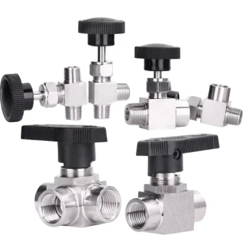
- 304 316 Stainless Steel High Vacuum Ball Stop Valve for Vacuum Systems
- Small Vacuum Heat Treat and Tungsten Wire Sintering Furnace
- Vacuum Heat Treat Sintering Furnace with Pressure for Vacuum Sintering
- Vacuum Heat Treat Sintering and Brazing Furnace
People Also Ask
- What is the role of a Vacuum Induction Melting furnace in Fe3Al/Cr3C2 preparation? Purity & Precision for Cladding
- What is the critical role of a Vacuum Induction Melting furnace in FeAl alloy prep? Achieve Ultra-High Purity Alloys
- Why is a Vacuum Induction Melting furnace (VIM) used for Cu-Zn-Al-Sn alloys? Achieve Precision Composition Control
- What is the role of VIM and directional solidification in aero-engine blade substrates? Engineering Extreme Durability
- What are the advantages of using a VIM furnace to control residual oxygen pressure? Achieve Superior Metal Uniformity